|
Executive Overview The motivation for developing higher density electronic packaging continues to be the market, primarily the high-volume cellular phone market. The consumer, after all, is expecting that each new generation of products furnish greater functionality, be smaller than its predecessor’s, provide higher performance and more memory for applications and data storage. There are two directions a company may choose when planning their product; expanded silicon integration (system-on-chip) or joining a number of existing silicon elements in a single package format (system-in-package). With volume manufacturing, product costs can be stabilized so that advanced IC package innovations become more available, even for other product segments. |
Vern Solberg, STC-Madison, Madison, WI USA
The increase in electronic functionality can be achieved through the development of more complex silicon integration but that route generally requires a great deal of capital resources and time. A leading semiconductor packaging company executive stated, "In general, functions that can economically be integrated should be integrated using system-on-chip." The key word is "economically," and this puts constraints on the suitable application for the SoC package. Although the system-on-chip (SoC) approach can reduce system size and increased functional performance, the complexity of the design process and sorting out access to intellectual property (IP) controlled by others can be costly. Even more significant, development cycle time for the custom silicon product may be several months to several years, likely causing conflict with the life cycles for most cell phone products.
 |
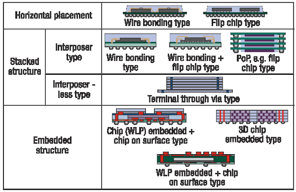
| Figure 1. Variations of current system-in-package methodologies. SOURCE: iNEMI 2009 Industry Roadmap |
To address the need for greater functionality quickly, a number of companies have already shifted away from single-die packaging and have adapted various forms of multiple-die system-in-package (SiP) innovations typical of those illustrated in Fig. 1. A market report prepared by Prismark identifies four categories of SiP:
• Modules: including LTCC and PCB (printed circuit board)-based modules that combine one or more uncased die and integrated and/or discrete passive components in a ball grid array (BGA), land grid array (LGA), or castellated joint package. The majority of high volume module designs are for RF applications, such as mobile phone power amplifier modules and Bluetooth modules.
• Multi-chip modules (MCMs): with multiple uncased die and optional passives in side-by-side and stacked die configurations with standard package outlines. Examples include graphics processor and memory MCMs as well as CPU and memory MCMs.
• 3D stacked-die packages: including any standard package outline with two to five (or more) vertically stacked devices with a lead-frame, PCB, or flex circuit base. The primary application is memory for mobile phones.
• 3D stacked package-on-package (PoP) and stacked package-in-package (PiP): PoP includes pre-packaged devices that are stacked on top of each other using lead-frame, PCB, and flex-based solutions. PiP includes stacked package configurations where one of the die stacks includes an over-molded package.
The first challenge for the package designer is to select the optimal SiP structure. For 2D applications, each die can be placed on the SiP interposer with either face-up (wire-bond) or face-down (flip-chip, stud-bump, or lead-bond). The module and MCM configurations are typically classified as a 2D structure and generally relies on ceramic, organic laminate or silicon as a base substrate to interconnect both incased and uncased devices. It has become more common for companies to use smaller passives and flip-chip mounting to reduce module size. In addition, many commercial component outlines have significantly decreased in size and advances in substrate manufacturing methodologies have enabled closer spacing between devices. A combination of high-density build-up fabrication technology along with the use of embedded passives can yield a very efficient 2D assembly as well.
The 2D package form factor, although ideally suitable for a wide number of applications, may not meet the small outline requirements demanded by wireless handset developers. Companies developing products for long-term high-volume application are adapting packaging methods that combine a number of functions within the confines of a single package outline. Stacking multiple die elements and/or joining individual package sections in a vertical configuration has proved to be a very efficient and economical format for minimizing package outlines. The multiple-die package is often proving superior to the system-on-chip alternative because it can economically integrate several different but complementary functions. The design of the 3D multiple die package, however, requires a clear understanding of the relationship between devices, the on-package interconnect requirements and ultimately, the interface between package and the interposer structure.
The benefit to the user is increased functionality in a smaller space, often two or three die are encased in a single, fine-pitch ball grid array (FBGA) package outline. The most efficient die-stack package assembly process utilizes die combinations with size variation that can be mounted sequentially in a pyramid fashion. When the same size die are stacked, the die must be individually mounted and wire-bonded before adding the next die in the stack. To clear the wire-bond loop on the lower die, a spacer must be provided between active die layers. The die-stack process allows the supplier to rapidly develop basic multiple-die combinations. Using the co-design methodology, supplier and user engineers can develop a product in a matter of weeks and optimize the overall system interconnect to minimize or eliminate package design re-spins that saves both hardware costs and design cycles.
Direct joining of bare die has evolved as viable process for same size die using through-silicon-vias (TSVs) to join one silicon layer to another. The process, most commonly employed for memory applications, enables the joining of several layers of very thin die elements into a single monolithic form factor. There are, however, significant drawbacks to die-stacking. Unless all of the unpackaged bare die are pre-tested and known to be good (KGD) before assembly, the multiple-die package yields may be well below the acceptable levels traditionally established for the single-die package.
Package stacking reduces risk
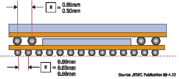
The package-on-package (PoP) innovations are proving to be far more predictable for a broad range of SiP applications. User companies have realized that complex mixed-technology functions can be produced with higher yield and more economically if the semiconductors are individually pre-packaged and tested before joining. The most common solution for PoP applications utilizes package sections designed around the JEDEC standard array packaging format (Fig. 2). Stacking pre-packaged die has less risk because the individual packages are fully tested before conversion to the stacked PoP format.
 |
| Figure 2. JEDEC Standard format for package-on-package components. SOURCE: JEDEC Publication 95-4.22 |
Acknowledgment
Bluetooth is a registered trademark of the Bluetooth Special Interest Group.
References:
- Prismark Report, 2009 SiP Roadmap.
- 2009 iNEMI Industry Roadmap, Component and Subsystem Technologies Section.
- IPC International Technology Roadmap for Electronics, 2008-2009, Part B, Technology Trends and Part D, Component Packaging.
- ITRS White Paper 19.0, The next Step in Assembly and Packaging: System Level Integration in the package (SiP).
- Yole Développement, 2009 Report, Memory Applications: Packaging and Integration Trends.
Biography
Vern Solberg is an independent technical consultant based in Madison, Wisconsin specializing in design and assembly process implementation for surface mount and microelectronic technologies;email [email protected].
More Solid State Technology Current Issue Articles
More Solid State Technology Archives Issue Articles

