|
Executive Overview We developed low-temperature, defect-free Cu-Cu direct bonding processes with high interfacial adhesion energies. The quantitative analyses of the interfacial adhesion energies and seam voids of Cu-Cu bonds performed with varying process parameters showed that bonding temperature and post-bond annealing have the most significant influence on bond properties. By optimizing experimental parameters, we could achieve, even with a short bonding time, sufficient interfacial adhesion energies (≥5 J/m2 for the subsequent processes such as grinding) with no interfacial seam voids. Post-bond annealing performed at 250-300°C drastically improves the interfacial adhesion energy. |
Bioh Kim, Thorsten Matthias, Erkan Cakmak, EV Group, Inc., Tempe, AZ USA; Eun-Jung Jang, Jae-Won Kim, Young-Bae Park, Andong National University, Andong, Korea
Through-silicon via (TSV) technology represents a system-level integration of planar devices that are stacked and interconnected in the z-direction. TSV integration enables the smallest form factor and highest performance due to the shortest and most plentiful interconnects between chips. Due mainly to the thermal budget of CMOS devices, the bonding processes compatible with TSV-interconnected CMOS wafers are limited only to direct oxide bonding, metal bonding (Cu-Cu or Cu-solder-Cu), adhesive bonding and various hybrids of those methods.
Among all, Cu-Cu direct bonding has several advantages over other bonding methods, which include lower electrical resistivity, better electromigration (EM) resistance and significantly reduced interconnect RC delay [1-2]. However, the reliable Cu-Cu bonding for most industrial applications comes only from high temperature, high pressure and long process time mainly because of its tendency to form a native oxide which deleterioiusly impacts device reliability. Presently, high process temperature is one of the major bottlenecks of Cu-Cu direct bonding because it can negatively influence device reliability and manufacturing yield. Typically, the industrial Cu-Cu bonding process is performed at ≥ 400°C, requiring over an hour of the total process time.
The ultimate goal of this work is to develop the low temperature Cu-Cu bonding process while maintaining strong bonding energies. As the first step, we focused on understanding the impact of varying process parameters, such as bonding temperature, chemical pre-treatment, pre-bond annealing and post-bond annealing, on the interfacial properties (voids and seams) and subsequent adhesion energies.
Quantitative analyses of Cu-Cu direct bonds
The quantitative analyses of interfacial adhesion energies and interfacial seam voids of Cu-Cu bonds were performed with varying process parameters, where the 4-point bending method was used to measure interfacial adhesion energies and a focused ion beam (FIB) was used to examine interfacial seam voids.
 |
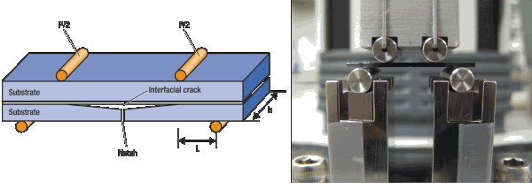
| Figure 1. Sample structure for 4-point bending test. |
Figure 1 illustrates the schematic of the sample for the 4-point bending experiment. The sample was placed between four load pins. A notch with the depth of 450µm was made on the bottom Si sample with a diamond blade to uniformly initiate the crack propagation during the bending test. The 4-point bending test is based on the fracture mechanics and used to calculate the interfacial adhesion energy between thin films, by measuring the energy release rate (G) which is required for a crack to propagate at the inner homogeneous material [3]. The sample has two elastic materials in a sandwich structure and the adhesion energy was measured during crack propagation at a constant moment, where a crack propagates along the weakest interface in multi-layers [4].
The interfacial adhesion energy, G (J/m2), was calculated using the following expression

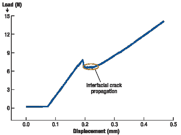
where v is Poisson’s ratio for an elastic material (Si wafer: 0.28), E is the elastic modulus of the elastic material (Si wafer: 130GPa), b and h are the width (3mm) and thickness of the specimen (500µm), respectively, P is the measured load, L is the distance between the inner and the outer loading points (5mm) and M is the moment defined as PL/2. In this experiment, the load cell was 20N, the loading speed was 0.08µm/s, and the distance between pins was 5mm. Figure 2 shows an example of the load-displacement curve of the Cu bonding layer from the 4-point bending test. The interfacial adhesion energy was obtained by using the plateau load in this graph.
 |
| Figure 2. Load-displacement curve for Cu-Cu layer from 4-point bending test. |
Experimental parameters
We used 100mm diameter blanket wafers with the thickness of 500µm. All the bonding experiments were performed using an EVG520 bonder at 25kN, 10-3Torr and N2 atmosphere. The vacuum level was initially maintained at 10-6Torr, but dropped to 10-3Torr when N2 was purged before the bonding process started.
Process parameters evaluated in this work include
• bonding temperature; 300, 350 and 400°C,
• chemical pre-treatments with a diluted acetic acid (80 vol.%); 1, 5, 10 and 15min,
• pre-bond annealing; 100 and 200°C for 15min at forming gas atmosphere, and
• post-bond annealing; 200, 250 and 300°C for 60min at N2 atmosphere.
Experimental results and discussion
Among all the tested conditions, bonding temperature and post-bond annealing showed the most significant influence on the interfacial adhesion energy and seam void formation. In comparison, the impacts of chemical pre-treatment and pre-bond annealing with the aforementioned conditions were much smaller. By adjusting those two experimental parameters, we could achieve, even with a short bonding time (30min), sufficient interfacial adhesion energies (≥ 5J/m2) with no interfacial voids. Post-bond processes such as grinding require typically at least 5J/m2 of the interfacial adhesion energy [5].
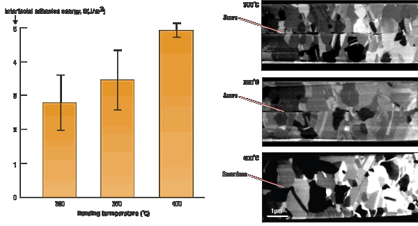
Bonding temperature effect. Wafers with 1.5µm thick, sputter-deposited Cu film on Si(100)/SiO2/Ta(25nm) were used for this experiment. Neither pre-bond surface treatment nor post-bond annealing was applied to samples. The pressure applied to the stack was 25kN and the bonding time was 30min, which is shorter than typical Cu-Cu bonding time (≥ 60min). With increasing bonding temperature, the interfacial bonding energy increased as illustrated in Fig. 3a. With the bonding temperature of 400°C, the minimal adhesion energy (5 J/m2) required for the post-bonding processes such as grinding was achieved. The original bond interface tended to disappear with increasing bonding temperature (Fig. 3b), which led to higher interfacial adhesion energy. All the fracture occurred through the Cu-Cu interfaces.
 |
| Figure 3. Interfacial properties as a function of bonding temperature; (a) interfacial adhesion energy and (b) microstructures of samples. |
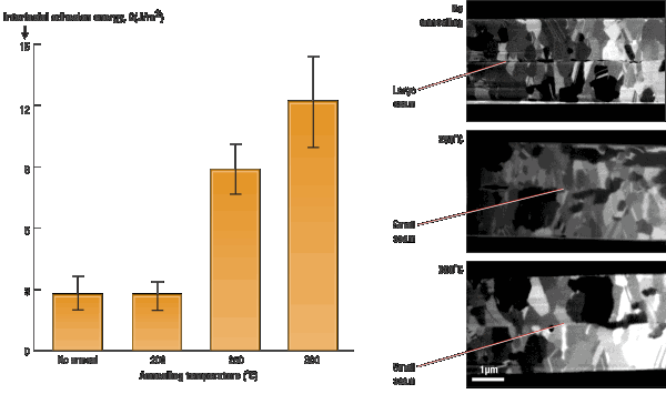
Post-bond annealing effect. All bonding tests were performed at 300°C and 25kN for 30min without any chemical pre-treatment or pre-bond annealing. Those samples were post-bond annealed at 200, 250 and 300°C, respectively, at N2 atmosphere for 60min. Figure 4a compares the microstructures of the samples annealed at different temperatures. In the case when post-bond annealing was not applied, the original interface or large seam was observed together with small voids because this bonding test was done at a low temperature with a short process time. With applying post-bond annealing at 200°C, no improvement in the interfacial properties was observed. After annealing either at 250°C or at 300°C, it was clearly observed that the interfacial seams between two layers decreased significantly. This means the post-bond annealing at 250-300°C can help Cu diffuse through the bond interface even when bonding is done at a low temperature (e.g., 300°C in this experiment). As illustrated in Fig. 4b, a decrease in the interfacial seam size resulted in higher bond strengths with increasing annealing temperature. In all cases the fracture occurred through the Cu-Cu interfaces.
 |
| Figure 4. Interfacial properties as a function of post-bond annealing temperature; (a) interfacial adhesion energy and (b) microstructures of samples. |
Post-bond annealing conditions evaluated in this experiment were not strong enough to fully drive the recrystallization reaction at the interface between two Cu films, but sufficient to drastically improve the interfacial properties. Further optimization of subsequent post-bond annealing conditions is ongoing to lower Cu-Cu bonding temperature under 200°C. If a long process time for post-bond annealing is concerned for volume production, a batch annealing process can be suggested after bonding wafers.
Conclusion
Cu-Cu thermo-compression bonding facilitates fine-pitch, high density stacking of various devices resulting in lower electrical resistance and higher mechanical strength. With varying process conditions, the quantitative analysis of the interfacial adhesion energy of Cu-Cu thermo-compression bonds was performed using the 4-point bending test and the interfacial properties such as voids and seams were also examined with FIB to correlate the relationship between the interfacial properties and resulting adhesion energies. The process conditions evaluated in this work include bonding temperature, chemical pre-treatment, pre-bond annealing and post-bond annealing.
Among all, bonding temperature and post-bond annealing have the most significant influence on bond properties. By optimizing experimental parameters, we could achieve, even with a short bonding time (30min), sufficient interfacial adhesion energies (≥5J/m2) with no interfacial voids. With increasing bonding temperature (300, 350 and 400°C), the interfacial adhesion energy increases and the original bond interface tends to disappear. The post-bond annealing performed at 250°C or 300°C under N2 atmosphere for 60min, even though thermo-compression bonding was done at a low temperature (300°C), drastically improves the interfacial adhesion energy (8.87–12.17J/m2) by more than three times.
Acknowledgments
The following were co-authors of this paper: Seungmin Hyun and Hak-Joo Lee of the Korea Institute of Machinery & Materials, Daejeon, Korea.
References
- A. Fan, A. Rahman, R. Reif, "Copper Wafer Bonding," Electrochem. and Solid-State Lett., 2, 534 (1999).
- S. I. Kim, C. W. Lee, "Nitrogen Impurity Effects of W–B–C–N Quaternary Thin-film for Diffusion Barrier for Cu Metallization," J. Korean Phys. Soc., 50, 489 (2007).
- R. Shaviv, S. Toham, P. Woytowitz, "Optimizing the Precision of the Four-point Bend Test for the Measurement of Thin-film Adhesion,, Microelectronic. Eng., 82, 99 (2005).
- H. Zhenyu, Z. Suo, X. Guanghai, H. Jun, J. H. Prevost, N. Sukumar, "Initiation and arrest of an interfacial crack in a four-point bend test," Eng. Fracture Mech., 72, 2584 (2005).
- R. Tadepalli, Ph. D. Thesis, "Characterization and Requirements for Cu-Cu Bonds for Three-dimensional Integrated Circuits," Massachusetts Institute of Technology (2007).
Contact author:
Bioh Kim is Global Business Development Manager at EV Group, Inc., 7700 S. River Parkway, Tempe, AZ 85284, USA; ph.: 480-294-9342; email [email protected].
More Solid State Technology Current Issue Articles
More Solid State Technology Archives Issue Articles

