|
Executive Overview As the semiconductor industry pushes the fundamental pitch of integrated circuits below the diffraction limits of 193nm immersion optics, lithographers have focused on developing double patterning-based approaches to bridge the gap until the insertion of EUV lithography. For logic applications where design flexibility is a concern, pitch-split double exposure (PSDE) technology such as litho-litho-etch (LLE) using resist-on-resist technology [1-3] and litho-etch-litho-etch (LELE) [4-6] are prominent techniques, although they magnify issues of overlay and CD control [7-12]. |
Venkat R. Nagaswami, Jaydeep Sinha, Sathish Veeraraghavan, Frank Laske, Pavel Izikson and John C. Robinson, KLA-Tencor Corp., Milpitas, CA
Overlay accuracy between the two patterns comprising the layer is generally considered the biggest challenge in PDSE. Several papers detail the mathematical relationships between CD uniformity (CDU) and overlay from which process tolerances can be derived [13]. Nominally, three independent components contribute to overall PDSE performance: first-exposure (L1) CDU, second-exposure (L2) CDU, and L2-to-L1 alignment. In the work reported in this article, a series of experiments and finite-element model (FEM) simulations were performed in order to investigate the magnitude of various contributors to overlay error in a representative PSDE process described previously [7]. The goal was to identify and prioritize areas of improvement within the PSDE process and evaluate the predictive capability of modeling software. An earlier version of this work was reported at the 6th International Symposium on Immersion Lithography Extensions, in November, 2009 [14].
Design of experiment
To study the various components of overlay error, a custom designed PDSE mask-set was fabricated using an electron beam mask writer containing test patterns, programmed defects, and various intra-field and inter-field alignment and registration marks. The alignment marks, split between the L1 and L2 masks, were designed to meet both mask registration metrology and wafer overlay metrology requirements. The test pattern contained cells of 11 x 14 rows and columns, and each cell contained 49 targets in each of 71 fields, approximately 24mm x 30mm in size. The L1 and L2 masks were used to create five PDSE wafers using a litho-freeze-litho approach detailed previously [8].
DPL overlay error
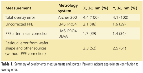
The overlay error between L2 and L1 exposures was measured for each of the five wafers using an Archer 200 metrology system and embedded targets. To estimate the contribution of mask pattern placement error to the overlay error, the same embedded targets were measured by an LMS IPRO4 metrology system. The results show a 3σ overlay error in X and Y of 4.4nm and 4.1nm, respectively, with a mean offset below 1nm. Wafer shape was also measured to quantity its contribution to the total overlay.
Pattern placement error (PPE) contribution
Pattern placement error (PPE) vector plots of the L1 and L2 reticles, shown in Fig. 1a and 1b, indicate the displacement of features relative to design coordinates. Software included with the PPE metrology system was used to determine the net PPE from the two layers, as shown in Fig. 1c.
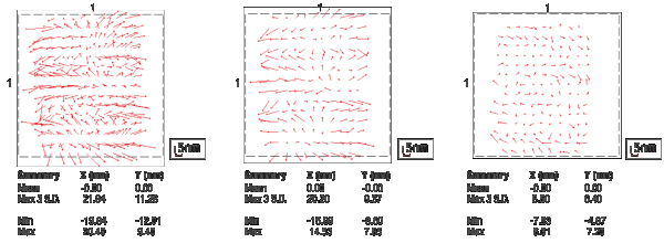 |
| Figure 1. Vector plots of pattern placement error for a) L1 and b) L2 masks; c) net results obtained from DEVA software. |
The magnitude of the net uncorrected PPE was found to be 8.5nm in X and 6.4nm in Y. Since L1 and L2 are 4X masks, this pattern placement error would translate to ~2.1nm in X and 1.6nm in Y on the wafer. These results suggest that the mask contributes significantly to overlay on the wafer, on the order of 40-50%. However, standard first-order corrections such as translation, magnification and orthogonality are correctable on the scanner. Using the PPE tool’s software to model ‘corrected’ PPE residuals reduced the errors to 6.6nm in X and 5.8nm in Y, which translate on the wafer to 1.7nm and 1.4nm, respectively. Third- and fifth-order corrections were also attempted but did not significantly improve the overlay residuals. The net corrected mask PPE contribution to the total overlay error is still significant: between 35% and 40%, even though the L1 and L2 reticles meet today’s ITRS reticle image placement specifications [15]. These results suggest that for PSDE, reticle image placement error can be a leading component in process variability and as such methodologies to deal with incoming variation must be developed.
Wafer shape contribution
Wafer shape is defined as the deviation of the surface of a wafer from a plane in its free-body state. The wafer is forced to undergo mechanical deformation when it is chucked flat in the stepper/scanner. This deformation causes the wafer topography to contract or expand radially and this in-plane distortion (IPD) may cause pattern shift [16] (Fig. 2). The linear component of the pattern shift can be corrected by the alignment metrology system in the stepper/scanner. However, any high frequency, non-linear pattern component can still contribute to overlay error (Fig. 3).
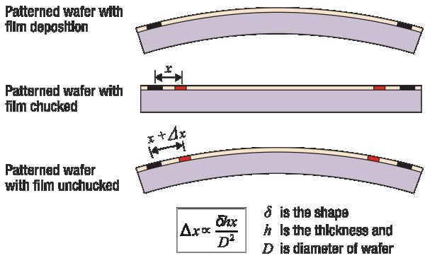 |
| Figure 2. The behavior of flattened wafer when chucked to stepper/scanner stage |
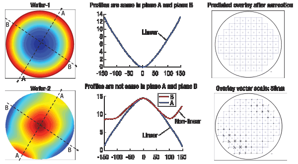 |
| Figure 3. Linear shape changes as exhibited by wafer-1 can be compensated by the scanner, but the high frequency shape contribution shown in wafer-2 would require dense high-order alignment / overlay correction in order to compensate for IPD resulting from chucking [11]. Note that these wafers are examples, not from this study. |
The shape of one of the five wafers was measured by a prototype interferometer. By assuming the change in wafer shape that occurred before and after the L2 exposure to be negligibly small, we modeled the shape data using a finite element method (FEM) to calculate the resulting IPD map across the wafer (Fig. 4). The wafer shape-induced IPD map shows increasing magnitude with wafer radius. The IPD deviates from linearity beyond a radial distance of 120mm, in the vicinity of the wafer edge. Similarly the overlay residual is larger (by 24% on average) in the region near the wafer edge. This observation supports the hypothesis that non-linear wafer shape may contribute significantly to overlay error.
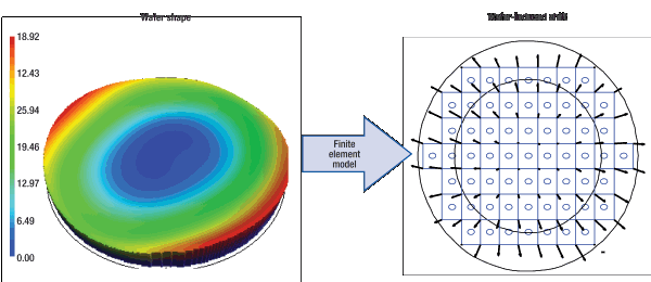 |
| Figure 4. Sample wafer from the experiment and the corresponding IPD prediction from the finite element model. |
The potential for wafer shape to contribute significantly to overlay error suggests that selecting wafers at the beginning of a process for geometry metrics such as flatness, edge roll-off (ERO) and wafer shape would minimize the impact on double-patterning overlay error.
Conclusion
Using a specially designed PSDE reticle set to print five wafers, we studied the contribution of pattern placement error and wafer shape to overlay error. Results are summarized in Table 1. We measured a total overlay error (3σ) of 4.4nm in X and 4.1nm in Y. We then measured the L1 and L2 masks’ pattern placement error and determined that PPE contributed significantly to PSDE overlay error (40-50%). By modeling we showed that if linear corrections were made to the PPE maps of each mask, thereby simulating scanner compensation during exposure, the contribution of PPE to overlay error would be reduced to about 35%.
We measured wafer shape on a prototype tool and used finite element analysis to show that the in-plane distortion caused by wafer shape effects correlates qualitatively to overlay error. In future studies, we plan to measure wafer shape before and after thin-film deposition and quantify the contribution of wafer shape changes to overlay error. In a typical CMOS process, the thin films exert a large amount of stress and the overlay impact due to high frequency, non-linear changes may be significant.
Our results suggest that wafer selection at the beginning of a process could help minimize the effects of shape changes during the wafer processing. Reduction of PPE contributions to overlay error can be accomplished by feed-forward of the PPE maps to the scanner and by tightening PPE metrics on incoming masks. The remainder residual error of about 2nm should be more than adequate to handle 2Xnm and 1Xnm design rules, according to industry guidelines and prevailing opinion.
Endnotes
An earlier version of this work was reported at the 6th International Symposium on Immersion Lithography Extensions, in November, 2009 [13]. Archer is a trademark of KLA-Tencor Corp.
References
1. G. Wakamatsu, Y. Anno, M. Hori, et al., "Double patterning process with freezing technique," Proc. SPIE, Vol. 7273, 72730B (2009).
2. M. Reilly, et al., "Evolution of thermal cure resist for double patterning applications," Proc. SPIE 7639, 76392W (2010).
3. K. Petrillo, M. Colburn, S. Dunn, et al., "Investigation of lithographic feature characteristics using UV cure as a pitch doubling stabilization technology for the 32nm node and beyond," Proc. SPIE, Vol. 7637 (2010).
4. K. Lai, S. Burns, S. Halle, et al., "32nm logic patterning options with immersion lithography," Proc. SPIE 6924, 69243C (2008).
5. M. Burkhardt,, et al., "Overcoming the challenges of 22nm node patterning through litho-design co-optimization," Proc. SPIE 7274, 727404 (2009).
6. L. Van Look, J. Bekaert, V. Truffert, et al., "Printing the metal and contact layers for the 32 and 22nm node: comparing positive and negative tone development process," Proc. SPIE 7640, 764011 (2010).
7. C.-S. Koay, S. Holmes, K. Petrillo, et al. "Evaluation of double-patterning techniques for advanced logic nodes," Proc. SPIE 7640, 764009 (2010).
8. S. Holmes, C.-S. Koay, K. Petrillo, et al., "Engine for characterization of defects, overlay, and critical dimension control for double exposure processes for advanced logic nodes," Proc. SPIE, Vol. 7273, 727305 (2009).
9. J. Finders, M. Dusa, B. Vleeming, et al., "Dense lines created by spacer DPT scheme: process control by local dose adjustment using advanced scanner control," Proc. SPIE 7274, 72740R (2009).
10. M. Colburn, et al., "Double Patterning Lithography Overlay Components," 6th Intl Symp. on Immersion Lithography Extensions, Prague, Nov., 2009.
11. S. Halle, D. Moore, C. Archie, et al., "Spatial signature in local overlay measurements: what CD-SEM can tell us and optical measurements cannot," Proc. SPIE 7638, 76381V (2010).
12. J. Finders, M. Dusa, B. Vleeming, et al., "Double patterning lithography for 32nm: critical dimensions uniformity and overlay control considerations," J. Micro/Nanolith. MEMS MOEMS, Vol. 8, 011002 (2009).
13. A. J. Hazelton, N. Magome, S. Wakamoto, et al., "Achieving overlay budgets for double patterning," Proc. SPIE, Vol. 7274, 72740X (2009).
14. V. Nagaswami, et al., "Double Patterning Lithography Overlay Components," 6th International Symp. on Immersion Lithography Extensions, Prague, November, 2009.
15. ITRS Litho Roadmap at http://www.itrs.net/Links/2009ITRS/2009Chapters_2009Tables/2009_Litho.pdf
16. K. Turner, et al., "Predicting distortions and overlay errors due to wafer deformation during chucking on lithography scanners," J. Micro/Nanolith. MEMS MOEMS 8(4), 043015 (2009).
Contact author
Venkat R. Nagaswami is patterning technology director at KLA-Tencor Corp., One Technology Drive, Milpitas, CA 95035; ph.: 408-875-3000; email [email protected]
More Solid State Technology Current Issue Articles
More Solid State Technology Archives Issue Articles

