 |
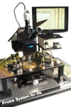
Manual Device Characterization |
 |
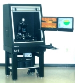
150 mm Semiautomatic System |
 |
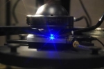
Optoelectronic Configuration |
 |
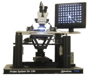
Double Sided Probe Configuration |
(August 11, 2010) — SemiProbe has developed proprietary technologies awarded a patent by the United States Patent and Trademark Office. The Probe System for Life allows the company and users to configure test and inspection systems that meet unique requirements usually served by custom products.
For traditional test systems, Probe System for Life allows the user to configure the station with exactly what they need and can budget for instead of a set configuration prepared by a probe system vendor. For facilities with multiple users, the system also allows the user to reconfigure the station in minutes for another application.
In addition to wafer testing, the system has been configured to test laser bars, singulated die, packaged parts, microfluidic slides, as well as device testing in controlled environments such as vacuum, cryogenic and ultra-high temperature (1,000°C). Special applications such as Double Sided Probing, Back Side Probing, Simultaneous Double Sided Probing and Visual Inspection have all been engineered and are available as standard components.
The Probe System for Life System allows users to perpetually upgrade their system as their needs change and budgets grow. Systems can be field upgraded from manual, to semi and fully automatic operation, in addition to changes in wafer size capability, environment, optics and instrument integration. Specific accessories to make probing easier for a specific application can also be added quickly and easily.
Since introducing the Probe System for Life, Semiprobe has sold systems to customers on 5 continents. Users completing a field upgrade to increase wafer size capability or automation often save up to 70% over the traditional requirement to start with a new probe system, according to the company.
SemiProbe is a global supplier of innovative probing and inspection equipment for microelectronics, photovoltaics, optoelectronics, MEMS, biotechnology, chemistry, microfluidics, and nanotechnology. More information about SemiProbe may be found at http://www.semiprobe.com
Follow Advanced Packaging on Twitter.com by clicking www.twitter.com/advpackaging. Or join our Facebook group

