January 19, 2011 — Dan Armbrust, president & CEO of SEMATECH, spoke about the role of collaboration in his SEMI Industry Strategy Symposium (1/9-1/12/11, Half Moon Bay, CA) presentation. Significant technology transitions (see table) facing the semiconductor industry include lithography (introduction of EUV), interconnects (TSVs and 3D packaging), and productivity (450mm wafer manufacturing). Additionally, disruptive technology in logic and memory devices will challenge the industry. In a podcast interview with Debra Vogler, senior technical editor, Armbrust sheds light on SEMATECH’s role in tackling these issues as well as the role governments can play.
Listen to Armbrust speak: Download (for iPhone/iPod users) or Play Now
Calling 450mm manufacturing "inevitable," Armbrust notes that "everyone is looking for a business model around 450mm wafer size introduction that would allow us to make investments with help from government entities."
|
||||||||||||||||||||||||||||||||||||||||||||||||||||||||||||
| Table. Major manufacturing technology transitions. Source: SEMATECH January 2011. | ||||||||||||||||||||||||||||||||||||||||||||||||||||||||||||
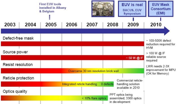
Metrology tools for extreme ultraviolet (EUV) lithography are another industry need that could benefit from governments’ support (Fig. 1). SEMATECH’s role is in channeling governments’ interest so that it’s a win-win for the industry as well as for specific regions that want to develop their work force and infrastructure, said Armbrust. SEMATECH provides the "forcing function" to find the gaps in each of the technology transitions and facilitate finding an industry consensus to address them.
 |
| Figure 1. EUV progress: critical enablers. Source: SEMATECH January 2011. |
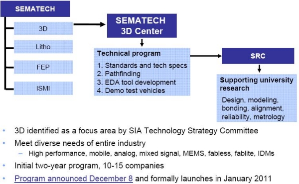
In the podcast, Armbrust also discusses the challenges associated with bringing 3D manufacturing and through silicon vias (TSVs) into volume production (Fig. 2). One application that Armbrust said would support 3D manufacturing (i.e., TSVs) in high volume is smart phones in the 2013 and beyond roadmap — the required data rate for these phones will need TSVs to enable the power reduction, as well as the space and cost savings.
 |
| Figure 2. 3D enablement program: SIA-SEMATECH-SRC. Source: SEMATECH January 2011. |
Subscribe to Solid State Technology/Advanced Packaging.
Follow Solid State Technology on Twitter.com via editors Pete Singer, twitter.com/PetesTweetsPW and Debra Vogler, twitter.com/dvogler_PV_semi.

