January 20, 2011 — Ionizers can improve wafer back- and frontside particle performance in physical vapor deposition (PVD) processing tools by removing surface charges that hold electrostatically adhered particles. Controlling surface charges on production wafers results in higher yields for chip manufacturers and improved tool performance. Viraj Pandit and Emery Kuo, Novellus Systems and Cheryl Avery, ION Systems show that the INOVA PVD system’s good particle performance (demonstrated on good quality wafers) is made more robust with an ionizer installation when marginal quality wafers are used.
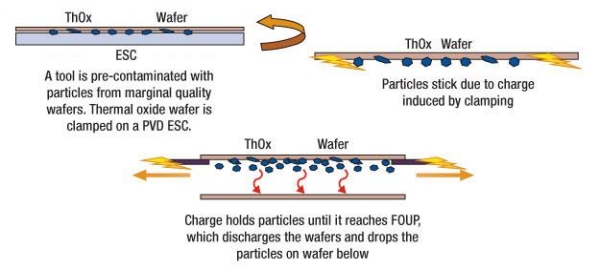 |
| Figure 1. Hypothesis of particle showering due to electrostatically adhered particles to thermal oxide wafers. |
The International Technology Roadmap for Semiconductors (ITRS) provides guidelines for both the number of allowable backside wafer particle adders and also the size of the adders. The size of particle adders identified as killer defects in the 2009 ITRS update [1] are 140nm on the back side and 25nm on the front side for back-end-of-line (BEOL), with stricter guidelines for front-end-of-line (FEOL). Because electrostatic attraction is known to cause both particle attraction and adhesion, the 2008 ITRS update [2] guides equipment manufacturers to limit the maximum static charges on wafer surfaces to a corresponding electric field of 70V/cm for the 65nm node, and 50V/cm for 45nm. Static charge audits performed in production fabs frequently report oxide wafer field voltages as high as 2kV/cm, much higher than the ITRS-recommended limits. Ionization is an industry-recognized method for neutralizing static charges in cleanrooms to reduce particles. In-tool ionization is a way to reduce static charge on the wafer to safe levels that will prevent the electrostatic attraction and subsequent particle adhesion.
The authors describe an in-tool study performed in a Novellus INOVA NExT tool that used ionizers to reduce backside particles [3]. Upon transfer to the FOUP, particles electrostatically adhered to the wafer back side were released onto the wafer located directly below the contaminated one. By using ionizers to neutralize the electrostatic charge prior to moving the wafer into the FOUP, showering and contamination were almost eliminated. The study looked at effects with different clamping voltages and methods of static discharge, including conductive cones and two ionizer types and locations.
SEM and EDX images of the particle adders on the cross-contaminated wafers showed silicon and oxygen signatures, indicating these particles were silicon oxide particles. In this study, the amount of particle adherence and showering is related to oxide thickness and wafer quality.
It was hypothesized that a tool, exposed to the marginal quality "dummy" wafers used for particle monitoring, becomes contaminated with small insulating particles. While particle monitoring wafers retain some residual charge after clamping in PVD modules, oxide wafers retain surface charge even longer, especially when the oxides are thick. The surface charges, which also exist on the back side of the wafer, electrostatically attract and hold some of these small insulative/dielectric particles. Oxide wafers in the tool thus act as particle getters and then carry particles to the FOUP, where the wafers are partially discharged through the static dissipative liner. The static charge reduction combined with FOUP movement causes the particles to overcome Vanderwaal’s forces and gravity, resulting in the loose particles showering on the wafer situated in a lower slot in the same FOUP, creating a particle excursion (Fig.1).
To test this hypothesis on the customer tool and validate the results, the study was performed at the customer site and also at Novellus. The wafers included both particle-/thickness-grade bare silicon wafers and Tox wafers (thermal oxide on both surfaces) with different oxide thickness values ranging from 1 to 20kA. The Novellus-recommended clamping voltage was kept unchanged in the mechanical wafer processing recipe (also known as per wafer pass [PWP] recipe). The difference between the PWP and in-film recipes is that the PWP recipe does not use any power (no DC, no RF).
Metrology measurements were performed using a Surfscan SP1. Electrical charge measurements were performed using a Faraday FOUP, manufactured by ION Systems. ION Systems Model 4632 Air-assist QuadBar (QuadBar), Model 5630 MP AeroBar, (MP AeroBar), and Model 5225 AeroBar (AeroBar) ionizers were used during this study.
When studying the physics of particle attraction, calculations show that the deposition velocities of submicron particles are controlled more by electrostatic forces than gravitational forces [4]. A stationary particle of 100nm diameter (d), having its center at a distance d away from the backside of a neutral oxide-wafer surface with a charge of just 100 electrons on the particle surface will be more affected by electrostatic forces than gravity. According to Coulomb’s law, electrostatic force (F) on a particle is
F = q2/(4πε0R2)
where, q is the amount of charge, ε0 is the permittivity of free space, and R is the distance of separation. Using image charge technique (R = 2d), the coulombic attractive force is 5.76 x 10⁻¹¹ N. The charge density on the particle surface is 3.2 × 10⁷ electrons/cm2.
Assuming that the 100nm-diameter particle with 100 surface electrons is made of SiO2 (bulk density 2634kg/m3), the gravitational force on this particle is 1.35 × 10⁻¹⁷ N. Since the gravitational force is much smaller than the calculated attractive force, the particle will get attracted to the surface.
In the frontend of a processing tool, charged particles that move near an already triboelectric charged SiO2 wafer backside have a high probability of being electrostatically attracted at high velocity rates and adhering to the wafer backside. The attractive force for smaller particles (smaller R) drastically increases as the image charge separation distance reduces. Thus, for smaller particle sizes, the binding force is even higher.
Ionizers neutralize all moving particles and wafer surfaces (including the wafer backside), reducing the chances of particle adhesion. In the case of already adhered particles on a wafer surface, ionizers can reduce the electrostatic forces holding these particles by effectively neutralizing charged surfaces. These loosened particles are then disrupted by gravity, wafer movement, and ionizer air-flow, allowing them to fall off before the wafer reaches the FOUP. To effectively remove particles that are adhered to a surface, surfaces must be neutralized as quickly as possible before the particles start to bond and exchange electrons.
Ionizers used to neutralize static charge should be chosen based on the application. Ionizers have different ion output densities and performance is measured by reporting the discharge time, the number of seconds required to reduce the potential of a charged plate monitor from ±1000 to 100V. The discharge time is dependent on ion density and external conditions such as air flow and humidity. Since a charged insulative (SiO2) wafer can have surface voltages in the kilovolts, an ionizer must have a high ion density to effectively reduce the charges to the SEMI spec values.
The study consisted of two phases: an experiment to identify the particle gettering and showering dependence on the oxide thickness, and testing to determine the effectiveness of conductive cones inside the process chamber and ionization in the mini-environment on reducing the static charge.
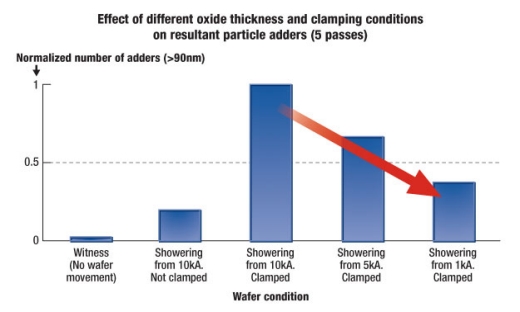 |
| Figure 2. Dependence of showering particle adders on wafer oxide thickness. A low witness value indicates clean mini-environment and good experimental control. Non-clamped low value indicates that the non-electrostatic particle adders were well contained. A lower value of particle adders for thinner oxide indicates thicker oxides’ higher capacity to hold more charges therefore attracting more particles on the wafer backside, and resulting in more showering on the wafer in the lower slot of the FOUP. |
The oxide thickness test was performed with oxide wafers separated by bare silicon particle-grade wafers (called the "showering" monitor wafers). The oxide thickness values used were 10, 5, and 1kA. Fig. 2 indicates a strong relationship between the charge-holding capacity of oxides, which is dependent on the oxide thickness, and particles showered by different oxide thicknesses. This observation supports the hypothesis.
The second phase of the test involved methods to reduce the static charge on the wafer and determine the resulting effect on particles. The first modification was to replace the ceramic cones contacting the wafer backside at a few locations in the load-lock module with customer-made doped zirconia conductive ceramic cones. The second hardware modification was to install three QuadBars to ionize the backside of the wafer when entering the mini-environment from the process. For a final production tool design, the QuadBars may be replaced with an MP AeroBar to reduce the ionizer footprint. The third modification was to install two AeroBars under the ULPA filter as topside ionizers.
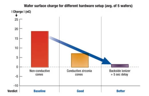 |
| Figure 3. Wafer surface charge reduction with different hardware modifications such as conductive ceramic cones and backside ionizer installation. |
As shown in Fig. 3, a baseline charge of ~18nC was reduced to 7nC by using conductive cones in the PVD tool load-locks. However, electrostatic attraction forces still existed and insufficient particle performance improvement was realized. The residual wafer charge was reduced to values below 2nC by using the backside ionizers and a 1min delay for testing purposes.
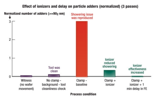 |
| Figure 4. Effect of ionizer assembly and delay on showering particle adders. |
The delay helped to effectively discharge the surface, allowing the adhered particles to fall off in the mini-environment instead of in the FOUP (Fig. 4). It was observed that, with this configuration, the wafer frontside did not receive the benefit of ions generated by the backside ionizers, therefore the topside AeroBars were also turned on, which reduced the wafer charges to zero or near-zero values.
 |
|
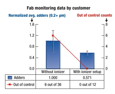
Figure 5. Particle monitoring data of a fab tool exposed to dummy wafers with marginal quality and during process wafer runs. |
Testing on an in-fab PVD tool showed that with both sets of ionizers installed, particle adders dropped from nearly 30 to less than 5 for multiple wafers. When the PVD tool was exposed to dummy wafers having marginal quality, the average adders were reduced by ~50% (Fig. 5); more importantly, though, the out-of-control (OoC) rate went down from 6 out of 36 to 0 out of 11 particle qualification data points. An approximately 60% particle reduction, even from low showering counts, was achieved by using the ionizers. Zero counts were obtained 50% of the time and the ionizer reduced backside showering consistently. Repeat measurements on a Novellus lab tool not exposed to marginal wafer quality confirmed this result with nearly a 50% reduction on 6 wafers (data not shown).
The average adders of multiple wafers were reduced significantly in the presence of both sets of ionizers with the addition of a delay to allow the particles to fall off before the wafer reached the FOUP. When only the backside ionizers were used, static charge built up in multiple other locations inside the mini-environment, which led to electrostatic forces keeping insulating particles mobile. The topside AeroBar ionizers provided full mini-environment coverage that ensured all of the surfaces and particles remained neutral. The presence of both top and bottom ionizers is recommended for optimized performance.
Conclusion
Backside wafer particle contamination can be reduced or even eliminated through the use of optimized topside and backside ionization. Electrostatically attached particles are removed before the wafer is put into the FOUP, and are effectively carried away in the laminar flow, preventing particle showering on the front side of wafers in lower slots. An effective reduction of wafer backside particles in a PVD tool can be achieved using optimized ionizer configurations.
REFERENCES:
1. ITRS Roadmap: http://www.itrs.net/Links/2006Update/FinalToPost/09_Interconnect2006Update.pdf Table 82a.
2. ITRS Roadmap Static Control: http://www.itrs.net/links/2005itrs/Linked%20Files/2005Files/Factory/Static%20Control%20Background05RevFINAL.doc 3. V. Pandit, E. Kuo; "Reduction of electrostatically adhered particles on wafer backside using ionizers," Advanced Semiconductor Manufacturing Conference (ASMC), 2010 IEEE/SEMI, pp.200-205, 11-13 July 2010.
4. D. W. Cooper, H.L. Wolfe, and R. J. Miller, "Electrostatic Removal of Particles From Surfaces", Particles on Surfaces 1, book, edited by K. L. Mittal, Plenum Press, New York & London, 1988.
Authors:
Viraj Pandit and Emery Kuo, Novellus Systems
Cheryl Avery, ION Systems
Subscribe to Solid State Technology/Advanced Packaging.
Follow Solid State Technology on Twitter.com via editors Pete Singer, twitter.com/PetesTweetsPW and Debra Vogler, twitter.com/dvogler_PV_semi.

