(January 10, 2010) — At the recent IEDM 2010 conference (12/6-12/8/10), Leti’s Olivier Faynot, Innovative Devices Laboratory leader, discussed invited paper #3.2 ("Planar fully-depleted SOI technology: a powerful architecture for the 20nm node and beyond") with Debra Vogler, senior technical editor.
Listen to Faynot’s talk: Download (for iPhone/iPod users) or Play Now
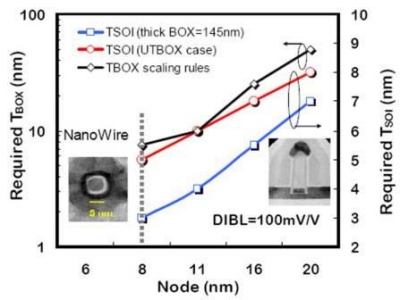
The use of fully depleted SOI (FDSOI) technology is of interest to Leti because some believe it will be a "serious alternative" to bulk technologies below 20nm. The group offered up a series of scaling rules for FDSOI devices down to the 8nm node (Fig. 1) and concluded that FDSOI can replace bulk devices below 20nm because of its electrostatic and matching capabilities.
 |
| Figure 1. Scaling rules of FDSOI devices down to the 8nm node. Below 8nm, nanowire-type devices should appear. SOURCE: Leti, IEDM 3.2 |
In the researchers’ work described in paper #3.2, they conclude that it is easier to integrate FDSOI than non-planer devices such as FinFETs. Faynot notes that the main advantages of FDSOI include driveability, scalability, and variability. The technology the group evaluated was undoped, ultra-thin FDSOI with a HK+MG stack.
The next step for the researchers is to enable circuit designers to build a platform — to that end, Leti is developing the applicable SPICE models. So far, the group has developed a model that simulates ultra-thin undoped channel devices with a possible back-bias effect. According to the paper, the model must include all SOI-specific effects such as, interface coupling, effects of the underlying substrate potential, the steep sub-threshold slope and the self-heating effect. The researchers reported that the model fit both static and dynamic performance.
 |
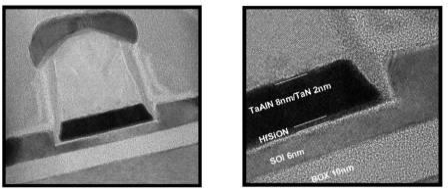
| Figure 2. TEM picture of LVT pMOSFET with 10nm thick BOX, 6nm thick SOI film, an indium GP, and a HfSiON/TaAlN/TaN gate stack (EOT=11.5Å). SOURCE: Leti, IEDM 3.4 |
Faynot also reviewed the significance of paper #3.4 ("Work-function engineering in gate first technology for multi-Vt dual-gate FDSOI CMOS on UTBOX [ultra-thin buried oxide]"). The researchers wanted to focus on the new materials needed to build low Vt transistors that are necessary for high-performance devices. The group co-integrated new materials with UTBOX SOI wafers to determine their suitability for high-performance devices (Fig. 2). They reported that multi-Vt solutions exist on undoped channel FDSOI using a gate-first approach and the integration of two different metal gates. The next step, noted Faynot, is co-integrating two metals to realize multi-Vt values on the same chip.
Subscribe to Solid State Technology/Advanced Packaging.
Follow Solid State Technology on Twitter.com via editors Pete Singer, twitter.com/PetesTweetsPW and Debra Vogler, twitter.com/dvogler_PV_semi.

