(January 6, 2011) — Cornell University researchers have unveiled striking, atomic-resolution details of what graphene "quilts" look like at the boundaries between patches, and have uncovered key insights into graphene’s electrical and mechanical properties.
Researchers focused on graphene — a one atom-thick sheet of carbon atoms bonded in a crystal lattice like a honeycomb or chicken wire — because of its electrical properties and potential to improve everything from solar cells to cellphone screens.
|
|
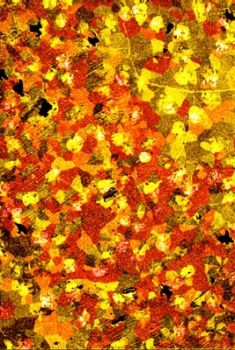
| Figure 1. A false-color microscopy image overlay depicting the shapes and lattice orientations of several grains in graphene. Source: Cornell |
But graphene doesn’t grow in perfect sheets. Rather, it develops in pieces that resemble patchwork quilts, where the honeycomb lattice meets up imperfectly. These "patches" meet at grain boundaries, and scientists had wondered whether these boundaries would allow the special properties of a perfect graphene crystal to transfer to the much larger quilt-like structures.
To study the material, the researchers grew graphene membranes on a copper substrate (a method devised by another group) but then conceived a novel way to peel them off as free-standing, atom-thick films.
|
|
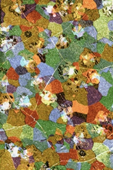
| Figure 2. Another graphene sheet with different lattice orientations. Source: Cornell |
Then, with diffraction imaging electron microscopy, they imaged the graphene by seeing how electrons bounced off at certain angles, and using a color to represent that angle. By overlaying different colors according to how the electrons bounced, they created an easy, efficient method of imaging the graphene grain boundaries according to their orientation. And as a bonus, their pictures took an artistic turn, reminding the scientists of patchwork quilts. (Published in Nature, Jan. 5, 2010.)
"You don’t want to look at the whole quilt by counting each thread. You want to stand back and see what it looks like on the bed. And so we developed a method that filters out the crystal information in a way that you don’t have to count every atom," said David Muller, professor of applied and engineering physics and co-director of the Kavli Institute at Cornell for Nanoscale Science.
Muller conducted the work with Paul McEuen, professor of physics and director of the Kavli Institute, and Kavli member Jiwoong Park, assistant professor of chemistry and chemical biology.
Further analysis revealed that growing larger grains (bigger patches) didn’t improve the electrical conductivity of the graphene, as was previously thought by materials scientists. Rather, it is impurities that sneak into the sheets that make the electrical properties fluctuate. This insight will lead scientists closer to the best ways to grow and use graphene.
The work was supported by the National Science Foundation through the Cornell Center for Materials Research and the Nanoscale Science and Engineering Initiative. The paper’s other contributors were: Pinshane Huang, Carlos Ruiz-Vargas, Arend van der Zande, William Whitney, Mark Levendorf, Shivank Garg, JonathanAlden and Ye Zhu, all from Cornell; Joshua Kevek, Oregon State University and Caleb Hustedt, Brigham Young University.
Follow Small Times on Twitter.com by clicking www.twitter.com/smalltimes. Or join our Facebook group


