January 24, 2011 — KLA-Tencor Corporation (NASDAQ: KLAC) debuted an automated inspection system for substrates and epitaxial wafers used in high-brightness LED (HBLED) manufacturing. The Candela 8620 provides automated defect inspection for LED materials such as gallium nitride, sapphire, and silicon carbide, enabling enhanced quality control of both opaque and transparent substrates, faster time-to-root cause, and improved metal organic chemical vapor deposition (MOCVD) reactor uptime and yield. Frank Burkeen, VP & GM of the Candela Division at KLA-Tencor, discusses the Candela 8620 inspection system.
Listen to Burkeen’s interview: Download (iPhone/iPod users) or Play Now
In the interview, Burkeen cites data made available in a Department of Energy (DOE) study and also addresses the importance of detecting process excursions faster. The differences between silicon CMOS manufacturing and LED manufacturing are also discussed.
 |
|
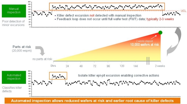
Figure 1. Example of the impact of faster excursion detection (manual inspection vs. automated inspection). SOURCE: KLA-Tencor |
With its proprietary optical design and detection technology, the Candela 8620 detects and classifies sub-micron defects that are not consistently identified by current inspection methods, according to KLAC. The recent DOE study is exciting, Burkeen says, because it shows that to achieve the cost reduction targets for SSD lighting to make it into the general lighting arena (about 10× cost reduction), process control, better methodology around defect inspection and root cause analysis is needed. Yield can be responsible for making up half of that cost difference.
In LED manufacturing, just growing the epi layers — the first part of the front-end process — accounts for about half of the value of the device, before you’ve even started fabricating the device, said Burkeen. According to industry sources, as HBLED manufacturers transition production to larger wafer sizes and introduce new patterned sapphire substrate (PSS) processes, the economic impact of resulting process-induced defects is estimated at millions of dollars in lost product revenue per year, and MOCVD epi process issues may result in as much as 40% of overall defect-induced yield loss. Quantum wells are constructed during the epi deposition and they determine the wavelength and luminosity of the device. "This is much different from silicon CMOS processing in which much of the value added occurs later in the process (as the structure is built with circuit lines)," observed Burkeen. Therefore, process control around an early step [in LED manufacturing], when the wafer is unpatterned, has a much greater significance than it would in CMOS manufacturing, he said (Fig. 1).
 |
|
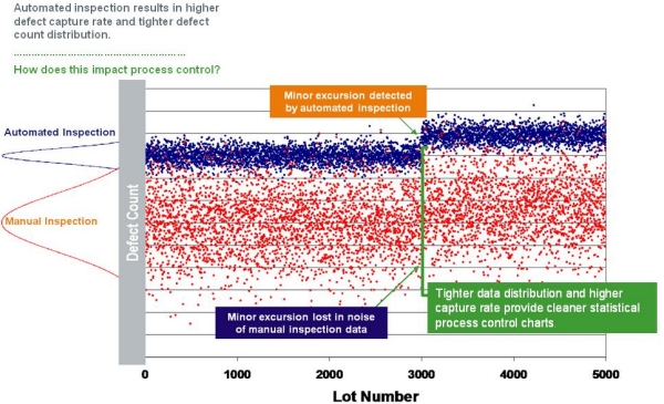
Figure 2. Excursion detection: impact of capture rate and tighter data distribution. SOURCE: KLA-Tencor |
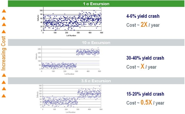
Burkeen also explained how automated inspection results in higher defect capture rate and a tighter defect count distribution (Fig. 2). Being able to produce a much tighter distribution with coverage of the full wafer gives you much more sensitivity to small excursions, noted Burkeen. An operator with manual inspection has virtually no sensitivity to a small excursion because of the area they are looking at, variability, etc. "Financially, a small excursion that is hard to catch, is really the most dangerous type for your financial performance as an LED manufacturer," said Burkeen (Fig. 3). LED substrate and epitaxy layers pose significant inspection challenges due to high levels of background signal and nuisance defects. The Candela 8620’s imaging and detection system is optimized to enhance the signal from relevant defects-of-interest while suppressing background noise. Aided by its multi-channel detection optics, the system additionally allows high purity classification of such defects, allowing comprehensive statistical process control of critical MOCVD processes.
 |
|
Figure 3. Economic impact of major vs. minor excursions. SOURCE: KLA-Tencor |
The Candela 8620 can detect:
- Substrate defects such as micro-scratces and micro-cracks which can create epi process defects and directly impact LED yield and reliability
- Defect sources from lithography and etch processes for patterned sapphire such as missing bumps and resist voids, resulting in epi defects or reduced lumen output
- Macro- and micro- defects in MOCVD processes, including hexagonal pits and bumps leading to electrical failure, and epi cracks which can adversely impact field reliability.
KLA-Tencor Corporation provides process control and yield management solutions with inspection and metrology technologies. These technologies serve the semiconductor, data storage, LED, photovoltaic, and other related nanoelectronics industries. Additional information may be found at www.klatencor.com. (KLAC-P)

