Authors: Jonathan Rullan1, Tadahiro Ishizaka2, Frank Cerio1, Shigeru Mizuno1, Yasushi Mizusawa2, Thomas Ponnuswamy3, Jon Reid3, Andrew McKerrow3, Chih-Chao Yang4.
1. TEL Technology Center, America, LLC, 255 Fuller Rd, Suite 244 Albany, NY 12203; 2. Tokyo Electron AT LTD. 650 Mituszawa, Hosaka-cho, Nirasaki City, Yamanashi 407-0192 JAPAN; 3. Novellus Systems, 11155 SW Leveton Drive, Tualatin, OR 97062; 4. IBM at Albany Nanotechnology Research Center, 255 Fuller Rd, Albany, NY 12203.
CVD ruthenium liners and direct seed (DS) copper provide lower resistance wiring compared to results using chemical vapor deposited (CVD) Ru and conventional physical vapor deposited (PVD) Cu seed for back end of line (BEOL) structures. Different annealing temperatures and simulated BEOL thermal stress builds were used to show the difference in resistance. The grain size was also compared to show that the Ru/DS process had larger grains than the Ru/flash-Cu (F-Cu) seed. To further show the advantage of the Ru/DS seed process as a solution for future generations, 2X nm trenches were shown to have complete gap fill, eliminating the need for conventional PVD Cu seed.
As Cu interconnect features continue to shrink, filling Cu interconnects with conventional PVD processes becomes more difficult to control, as a result of variability of step coverage and overhang of the Cu seed. The ability to deposit thin CVD Ru liners has been evaluated in BEOL metallization schemes and has been demonstrated to be a potential candidate for replacing PVD-based TaN/Ta/Cu low-k technology [1,2]. Ru/TaN has also shown to be a good diffusion barrier, providing low contact resistance, adhesion strength > 20J/m2 to Cu, and gap fill extendibility to 15nm contact plugs [1,3]. All of the above has been demonstrated using a conventional PVD Cu seed.
As a result of its noble characteristics, Ru provides a more suitable metal surface than traditional liners for direct electrodeposition of a Cu seed layer. While uniform Cu electrodeposition on thin Ru films in traditional electrofill baths is limited by terminal effect and nucleation issues, a new electrodeposition process called Direct Seed has been developed to provide high nucleation density and uniform across-wafer Cu films without overhang [4, 5].
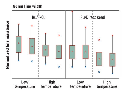 |
| Figure 1. Line resistance for an 80nm wide line with Ru/F-Cu and Ru/DS. |
Experimental
A 2nm CVD Ru liner was deposited using a 300mm system that also contained degas, Ar sputter pre-clean, PVD Ta, and PVD Cu. The CVD Ru liner had a split on the Cu seed layer, either a PVD F-Cu layer (10nm) or a DS Cu process (<10nm). Both Ru/Cu seed splits were processed on a plating system containing both the direct seed and conventional plating processes. The first set of patterned wafers was fabricated using a test structure providing 80nm single damascene Cu M1 line with dense dielectric. Electrical and transmission electron microscope (TEM) cross sections were taken to provide resistivity and grain analysis information. The second set of wafers consisted of a 45nm Cu low-k integration node where the wafers were subjected to a BEOL thermal stress. The BEOL thermal stress was equivalent to 6 BEOL metal levels. The third set of wafers deposited were backfilled with TEOS to reduce the CD of the trenches to 2Xnm node level.
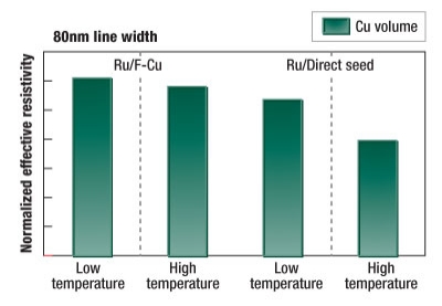 |
| Figure 2. Cu volume effective resistivity for an 80nm line with Ru/F-Cu and Ru/DS. |
Results and discussion
Electrical and grain measurements. The electrical measurement results in Fig. 1 show the line resistance of the Cu line following low- and high-temperature annealing and chemical mechanical planarization (CMP). The normalized line resistance of the 80nm lines shows that the Ru/Cu-DS process yields a ~10% decrease in line resistance compared to the Ru/F-Cu process for both annealing conditions. To verify that the line resistance is not an effect of CMP height difference, the effective resistivity of the Cu volume was taken of the tested line. When calculating the effective resistivity of the Cu volume, only the cross-sectional area of the Cu is used to calculate the resistivity of the tested line. The comparison shows that the Ru/DS had a lower resistivity by 5-10% compared to the Ru/F-Cu (Fig. 2). The lower resistivity indicates that the Cu grains for the Ru/DS may have been able to achieve a larger size, which would be ideal for low-resistance and high-reliability Cu wires.
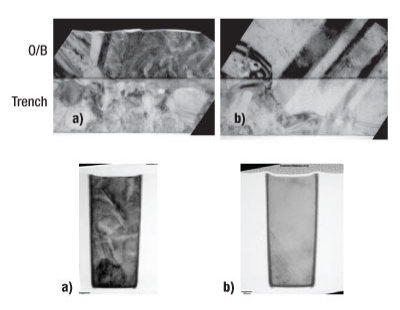 |
| Figure 3. Longitudinal and transverse TEM micrographs of a (a) Ru/F-Cu and (b) Ru DS process annealed at low temperatures. |
A comparison of the Cu grains between the Ru/F-Cu and those deposited with Ru/DS is shown in Fig. 3. The longitudinal and transverse TEM sections show that the Cu grains for the Ru/DS process are larger than for the Ru/F-Cu process. The Ru/DS process could yield larger grains because the Cu grains inside the trench more readily recrystallize to form a large grain that spans the overburden and the interior of the trench. The Ru/Cu-F process had negligible Cu grain growth, as seen by the TEM image.
|
Ru/F-Cu |
Ru/DS |
|
|
|
Average grain area (nm2) |
Average grain area (nm2) |
| Trench 1 |
1246.38 |
3609.33 |
| Trench 2 |
1974.70 |
1939.76 |
| Trench 3 |
2372.35 |
2190.22 |
| Trench 4 |
1690.43 |
2825.96 |
| Trench 5 |
1653.31 |
2593.57 |
| Total average grain area |
1750.67 |
2455.95 |
| Average grain diameter |
47.20nm |
55.9nm |
Measurements of the Cu grain size of the Ru/F-Cu and Ru/DS were analyzed and the results are shown in Table 1. The grains were measured by outlining the grains and calculating the area of the grain inside the trench. The average area was then used to calculate what the average grain size is inside the trench. The Ru/DS process data shows it to have 13% larger Cu grains than the Ru/F-Cu process.
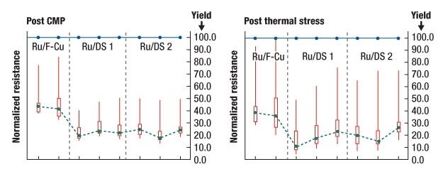 |
| Figure 4. Line resistance measurements for a Cu line before and after a 6 level BEOL thermal stress. |
To verify that the Ru/DS process maintains its lower resistance, the line resistance was measured after being thermally stressed. The thermal stress process mimics what a Cu wire would endure during subsequent builds of an interconnect chip. In Fig. 4, the Ru/DS process is shown to have a lower resistance than Ru/F-Cu initially after CMP. After the thermal stress, the resistance remained lower for the Ru/DS process by 10%. DS 1 and DS 2 represent the different seed thicknesses that were used. Both DS 1 and DS 2 had a thickness less than <10nm.
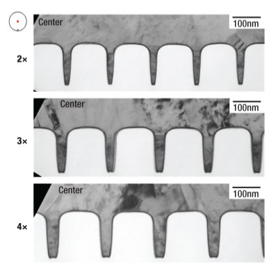 |
| Figure 5. Void free Cu fill for 2X, 3X, and 4Xnm trench dimensions. |
2Xnm node gap fill. For deposition processes to be accepted as a viable method for Cu interconnects in future generations, gap fill extendibility must be accomplished. Fig. 5 shows the gap fill at the center of a 300mm wafer for a 2X-4Xnm Cu wire. All of the sections show a void-free fill using a 2nm CVD Ru liner and 2.5nm Direct Seed Cu.
Conclusion
CVD Ru liner and Direct Seed Cu have been shown to have low resistance wiring compared to the more conventional CVD Ru liner and PVD Cu seed. The grain analysis of the Cu shows that the low resistance is due to the grains being larger for the CVD Ru and Direct Seed Cu. The combination of the two processes, along with its 2Xnm void free gap fill capability, shows that this technology is viable for providing low resistance wiring for current and future node levels.
References
1. C. C. Yang, et al., IEEE International Interconnect Technology Conference, 187 (2006)
2. F. Gstrein, et al., Proceedings Advanced Metallization Conference, 19 (2007)
3. S.-C. Seo, et al., IEEE International Interconnect Technology Conference, 8 (2009)
4. T. Ponnuswamy, et al, Proceedings Advance Metallization Conference, 15 (2008)
5. T. Ponnusawamy, S. Park, and J. Reid Proceedings Advanced Metallization Conference, 17 (2007)
Jonathan Rullan may be contacted at phone (518) 292-4221; [email protected]
Subscribe to Solid State Technology/Advanced Packaging.
Follow Solid State Technology on Twitter.com via editors Pete Singer, twitter.com/PetesTweetsPW and Debra Vogler, twitter.com/dvogler_PV_semi.

