(January 10, 2011) — During IEDM 2010 (12/6-12/8/10, San Francisco, CA), Debra Vogler, senior technical editor, had the opportunity to discuss scaling strategies with Glen Wilk, senior director, ALD & Epi products, Thermal Products Business Unit, at ASM America. For the near-term, i.e., extending scaling for one or possibly two more generations below 22nm, Wilk is keen on using materials modification to do the job. He views it as a simple near-term solution from a manufacturing standpoint, given the semiconductor industry’s experience with hafnium oxide (HfO), which is already in production.
 Listen to Wilk’s talk: Download (for iPhone/iPod users) or Play Now
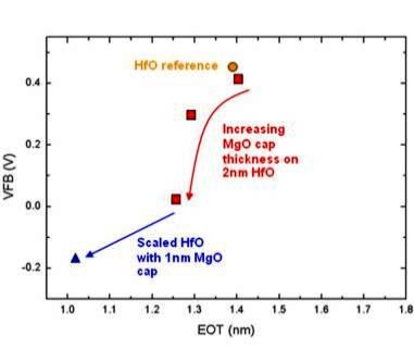
Wilk says that one can put a capping layer of another material on top of hafnium oxide to obtain a higher k value without degrading leakage, reliability, etc. (see the figure). The capping layer would have to be very thin and very controlled, with a thickness between 2 and 4Å, he told Solid State Technology. The materials used for the layers could be magnesium oxide or titanium oxide. During subsequent thermal processing, the magnesium or titanium ions would diffuse into the hafnium oxide, thereby modifying the network or provide a dielectric constant of their own, which would result in an increase of the effective k value of the stack.
 |
|
Figure. HfO/MgO stack vs. pure HfO. One method of EOT scaling is to deposit a cap layer, in this case MgO, on top of a standard HfO high-k gate dielectric. A subsequent anneal causes Mg diffusion into the interlayer, increasing the effective k value. The graph shows up to 2-3Å EOT reduction by increasing MgO cap layer thickness, with up to 550mV Vt shift. SOURCE: ASM |
Wilk cautions that it is important to consider implications of adding such layers (e.g., higher leakage currents, reliability). "It’s very important to do the right materials screening up front, whether it be from an electro-negativity standpoint or a thermo-chemical standpoint to ensure stability, compatibility, and desired properties," said Wilk. "Once we diffuse these materials into the stack, they can diffuse down toward the interface, increase the k value of the SiO2 layer, and thereby increase the effective k value of the stack."
He added that, by tailoring the dopant profile so there isn’t too much at the bottom interface, undesirable scattering phenomena or reliability impacts can be avoided. "I really do see that as the most viable approach — where we still maintain the basic hafnium oxide layer that everyone has put a lot of effort into processing — but just modify it with a few other elements to enable scaling without having to rework the entire process flow." Of course, the approaches to changing the device (FinFET, FDSOI, etc.) will continue because scaling has to happen on a continuing basis, observed Wilk, "but I really see materials modification as a near-term solution to enable a generation or two past 22nm."
Subscribe to Solid State Technology/Advanced Packaging.
Follow Solid State Technology on Twitter.com via editors Pete Singer, twitter.com/PetesTweetsPW and Debra Vogler, twitter.com/dvogler_PV_semi.

