January 13, 2011 — Yole Développement released details of its upcoming report, MEMS Manufacturing & Packaging. This report analyzes the main MEMS manufacturing evolution. MEMS drivers include size, cost, and performance, though in different ways than ICs. New MEMS manufacturing and packaging technologies and specific materials are necessary.
"With this report, our aim is to provide understanding of current challenges of MEMS manufacturing, packaging & materials. For each MEMS manufacturing step, bottlenecks and challenges are highlighted," explained Dr Eric Mounier, project manager at Yole Développement. Yole Développement’s approach is to analyze the MEMS industry evolution, per MEMS devices (inertial MEMS, magnetometers, pressure sensors, etc). Technical & market data covers the period 2000-2020. This study includes cost analysis, technical trends, impact on MEMS equipment & materials, manufacturing tools (DRIE, sacrificial release, etc), and engineered wafers & materials.
 |
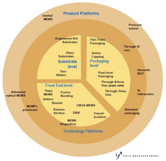
| Figure. Example of different MEMS manufacturing & packaging trends analyzed in the report “MEMS Manufacturing & Packaging” Source: Yole. |
Although MEMS technologies have not been driven by the same size demands as ICs, MEMS manufacturing is not just standing still. The fast growing MEMS markets, now led by consumer applications, are:
- Size-drive: for demanding consumer applications like smart phones and laptops
- Performance-driven: for high-end applications like aerospace
- Cost-driven: for high-volume applications like cell phones, automotive and game consoles
New MEMS manufacturing and packaging technologies and specific materials are necessary for solving these issues. Yole Développement’s report highlights the future challenges for MEMS production and packaging. From bulk micromachining to surface micromachining and then to SOI, MEMS technology has been following a well-defined evolutionary technical roadmap with 3D integration being the next possible step. The report includes manufacturing trends for the different MEMS devices in terms of processes, new packaging approaches, 3D integration, CMOS MEMS integration, new materials such as structured wafers, and more.
MEMS processes are analyzed at:
- The substrate level: engineered SOI, glass, thin wafers
- Front End level: piezo materials, getters, bonding, resists, CMOS MEMS, release stiction, DRIE, singulation, lithography, etching, sacrificial release, CAD tools
- The packaging level: thin film packaging, active capping, pixel-level packaging, through glass vias, through Si vias
- Technology platforms: TSV, hermetic WLP, interposer, standard packaging, MUMPS process, testing
This report analyzes the current major MEMS manufacturing trends and presents some clues for understanding the next evolution in terms of die size, cost, packaging. Among other MEMS technologies to watch for the future, Yole identified:
- At the substrate level: SOI, glass, thin wafers;
- At MEMS die level: getters, fusion bonding, release stiction, singulation, CMOS MEMS, DRIE, trench isolation;
- At the packaging level: TGV, TSV, pixel-level packaging, thin film capping, active capping.
For all the analyzed MEMS technologies, wafer forecasts 2009-2015 by type of step (DRIE, wafer bonding, sacrificial etch, through Si vias, thin films packaging, CMOS MEMS, thin wafers) are estimated.
| Companies cited in the MEMS report: |
| 36Deg, Accretech, AD, Aichi Steel, Air Products, AKM, Akustica, ALSI, Amkor, AML, APM, ASE, ASML, AST, Avago, Aviza, Ayumi, Bal-Tec, Baolab, Berliner Glass, BOC Edwards, Bosch, Brewer, Coventor, Dalsa, Dicon, Discera, Disco, Elpida, Entrepix, ePack, Epcos, EVG, FhG ISiT, FLIR, FocusTest, Freescale, FSI, Hamamatsu, Hitachi Metals, HP, IBM, IDEX, Idonus, Ikonics, IMT, Infineon, Invensense, Ixmotion, JDSU, Kionix, Knowles, LAM Research, Lemoptix, Leti, Lumedyne, Memscap, Memscore, Memsic, Memsstar, Memstech, MEMTronics, Micralyne, Micro Devices Laboratory, Microstaq, Mitsubishi Electric, Nanoplas, NEC Schott, NeoPhotonics, NovioMEMS, Okmetic, Omron, Panasonic Factory Solutions, Penta Technology, piezoVolume, Plan Optik, Polight, Primaxx, QinetiQ, QMT, RFMD, SAES, Samsung, Sandia National Labs, Santec, Semitool, Sensonor, Shell, Silex, Silicon Clocks, SiTime, Solidus Technologies, SPEA, Sporian Microsystems, STM, STPS, SUSS MicroTec, Tango, Tecnisco, Tegal, TEL, TI, TMT, TopCon, Toshiba, Tousimis, Tronics’, TSMC, Ulcoat, Ulis, UltraTechSteppers, Ulvac, Umicore, Veratag, Visera, Vi Technology, VTI, Xactix, XFAB, Xintec. |
DRIE and wafer bonders are the technologies subject to major evolution. "Both technologies are increasingly used for 3D TSV in the mainstream semiconductor business. Wafer bonding is the direct competitor to the CMOS MEMS approach," says Dr Eric Mounier. For example, microbolometer players are more and more considering a wafer bonding approach to stack the MEMS to the ROIC wafer.
CMOS MEMS is likely to be restricted to very specific applications where MEMS arrays will need very close electronic processing. For all other cases, it will depend on MEMS product cycle time, flexibility, cost, integration, market demand and power consumption.
In 2011, simplification of manufacturing remains an objective: Yole Développement’s MEMS law of "One product, one process, one package" still rules. Will it still rule in 2020? The current work on technology and product platforms aims to overcome Yole Développement’s MEMS law. But this approach will be custom-made standard processes. By 2020, it is likely that MEMS fabs will have developed internal standard process blocks, but with fab-specific standard tools. The technology/product platforms currently proposed by some MEMS foundries are an interesting approach. Technology platforms can be used to create their own product platform.
Dr. Eric Mounier has a PhD in microelectronics from the INPG in Grenoble and is in charge of market analysis for MEMS, equipment & material. The report, "MEMS Manufacturing & Packaging," will be available in February 2011. Yole Développement is a group of companies providing market research, technology analysis, strategy consulting, media and finance services. More information is available at www.yole.fr
Follow Small Times on Twitter.com by clicking www.twitter.com/smalltimes. Or join our Facebook group

