by Michael A. Fury, Techcet Group
January 17, 2011 – SEMI’s Strategic Materials Conference (SMC 2011) continued on Day 2 with introductory remarks specific to the electronic materials industry. This year’s theme was Material Innovation: Catalyst for Success. Two new features were introduced this year to facilitate some real time online dialog as well as ongoing discussions beyond the life of the meeting itself: one is the Electronic Materials Information group which has been created on LinkedIn and is open to everyone; the other is Techcet’s Electronic Materials Information Conference site, also open to everyone. The LinkedIn function provides excellent broad networking communication but limits the length of individual messages to 200 characters, plus an optional web link. The Techcet site facilitates full discussions with no length restriction. We hope readers in the electronic materials field will participate in both forums and keep discussions robust not only during conferences, but throughout the year.
The opening keynote for SMC 2011 was delivered by Nobu Koshiba, president of JSR Corp., speaking on semiconductor technology trends, challenges and opportunities. The consolidation of chip manufacturers (i.e. fewer customers) is a business challenge in its own right that is further compounded by the fact that the next several nodes will be driven by new device architectures, over which materials suppliers have no control and limited insight, he said. The focus for high-volume materials will shift to analog an power devices. New CMOS materials being developed have no guarantee of longevity beyond the node for which they are developed, decreasing the return on R&D investment.
A different perspective on semiconductor technology trends was delivered by Gary Patton, IBM’s VP of SRDC. He asserted that the three-way collaboration of fabs with materials & equipment suppliers is the only way that the Roadmap can be realized. Traditional scaling has run out of steam; only a combination of material and structure changes can facilitate progress. The ruling mantra will be atomic level in deposition, patterning, etching, cleaning and planarization. IBM has ~30 ongoing joint development programs in Albany with another ~30 already completed. Success stories include 2nd generation immersion litho for 28nm; topcoat for immersion litho to prevent resist & lens contamination by the fluid layer, with JSR; and source mask optimization to enable pattern resolution to 20nm, with ASML, Toppan, & Mentor Graphics. Extreme ultraviolet (EUV) lithography is critical to recover the optical k1 factor that degrades from 22nm to 15nm to the extent that double patterning is required, yet is itself not extendible. His roadmap of future device structures showed proof of concept devices to 3nm. A critical high implant dose resist strip was co-developed with ATMI. Copper contacts with a Ru barrier have been implemented on a 0.1μm2 6T-SRAM cell, breaking the paradigm that presumed the perpetual use of tungsten for the contact level.
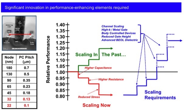 |
| CMOS scaling realities: Pitch degradation. |
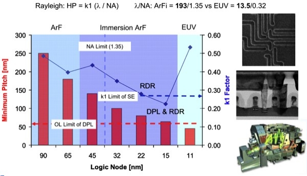 |
| EUV lithography: The promise of high k1 imaging. |
Redirecting the group’s focus, Andrew Thompson, co-founder and CEO of Proteus Biomedical, noted that the medical services industry does not serve as many as 85% of the global population. Only about 3.5B people on Planet Earth wear shoes — but 4.5B own cell phones, even though a vast majority of them earn less than $10 per day. Underlying this is the notion that individuals now hold more computing power than corporations and governments. The cost structure for medical enterprises has been built around the ability of the richest 10% to pay, whereas electronics innovation is underwritten by the richest but successfully addresses the ability to pay for the remainder.
| Revenue source | Medtronic | Novartis | Intel |
| ROW | 14% | 18% | 70% |
| Europe | 24% | 43% | 15% |
| USA | 62% | 40% | 15% |
The system uses edible electronics incorporated into the patient’s pills that, when ingested, transmit information to an external band-aid worn on the skin, which in turn transmits pill and vital sign data to a cell phone which then is made accessible to caretakers. ON Semiconductor is the primary partner for both the ingestible and wearable electronic components. Myfortic and Metformin are two of the drugs slated for initial commercialization; approval is well underway by the FDA and its European counterpart. The pharmaceuticals industry is $750B in 2010, but Morgan Stanley projects $2.0T in 2020 for this sort of intelligent pharmaceuticals, based on an electronics industry cost structure rather than traditional big pharma. Thompson’s vision is to bring affordable health care to everyone using technology. The ingested component is a silicon grain powered by a Cu and Mg bimetallic couple that is activated by body fluids. The digitally encoded data presents itself as a dipole that is detected by the band-aid. There is no powered RF involved until the data is transmitted beyond the band-aid. Product authentication is an additional benefit of this technology. In Nigeria, 80% of the pills taken are counterfeit or just plain fake; in China, one pill in seven is fake. The social implications of this technology and of changing the pharmaceutical business paradigm are huge.
Returning to somewhat more traditional device manufacturing and material technologies, Jae Hyun Kim, principal engineer at Samsung brought us the perspective of this leading manufacturer. Major upcoming innovations supported include 3D integration, EUV lithography, and capacitor dielectric competition between HfO2, ZrO2 and other high-k materials. Packaging density demand for 2012 will be up 3× for DRAM and 8× for Flash. Several examples emphasized the importance of analytical and characterization advances concurrent with technology advances, including rapid QC protocols. Their four pillars for resource conservation are recycle, reuse, reduce and refuse (eliminate processes). [Note that their 4 R’s are more correct that the traditional American 3 R’s, of which one is actually a W and which requires an apostrophe for ‘Rithmatic. Is this creativity or just marginal education?]
Blizzards in NY deprived us of a presentation from Bryan Rice, director of lithography at SEMATECH, on advanced lithography challenges (current and future). We hope to hear from him on this subject in the near future, before the challenges change — again. I’m pretty sure that snow was a challenge not included in his presentation.
Venturing into the More than Moore realm, mc10 CEO David Icke introduced us to high-performance conformal electronics. Venture-backed mc10 was co-founded by Prof. John Rogers at UIUC, who was originally scheduled to speak. The common theme is to leverage the performance of conventional silicon ICs into conformal and bio-inspired environments. David made the point that such technology represents a strategic direction for some electronic packaging applications. The technology is based on the flexibility of single crystal silicon that manifests when the material is sufficiently thin. Straightforward wet etch undercut is the production tool. Applying this flexible silicon to polymer, fabric or skins is managed using ‘accordion physics’ that tolerates 70% substrate strain while only imposing 0.2% strain on the metal interconnects between silicon features, and 0.15% strain on the silicon itself. Maintaining biocompatibility enables a host of medical applications, including optoelectronic catheters, trauma monitors in military helmets, temporary tattoos for vital sign monitoring, and a direct brain-computer interface. FDA certification aside, there is no fundamental cost hurdle anticipated in scaling up the technology.
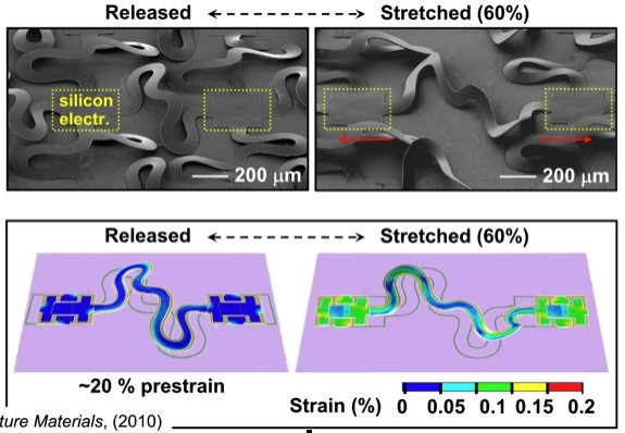 |
| Serpentine mesh interconnects. (Source: Nature Materials) |
Moving into semiconductor adjacencies, Joe Berwind, principal at Alternative Energy Investing, led us off with a discussion on grid parity, levelized cost of energy (LCOE), and the PV supply chain. Typical grid parity projections do not take into account the specific cell costs and performance and durability variations among the different PV technologies being commercialized. LCOE calculations normalize the effects of government subsidies, enabling more functional comparisons between regions:
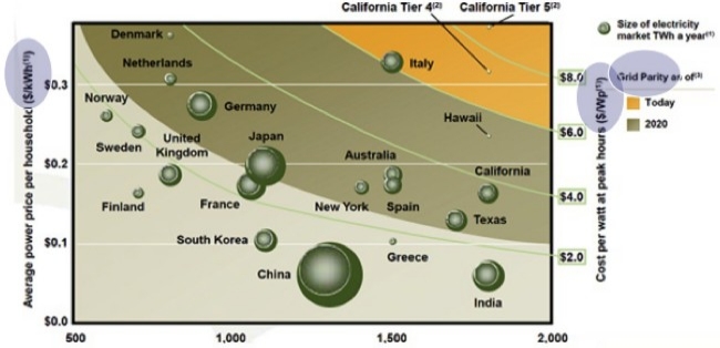 |
| Solar adoption/ growth trends by region, with grid-parity projections. (Source: Heliovolt) |
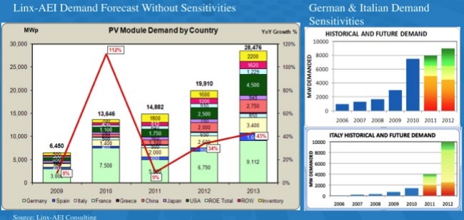
On the other hand, government subsidies play a tremendous role in accurate forecasting for PV silicon demand, but are frequently taken into account inadequately:
A technology overview of PV was provided by Rommel Noufi, principal scientist and PV group manager at NREL, focusing on high-efficiency CIGS solar cells. Thin-film PV share is 17% globally (62% in US), projected to be 25%-30% by 2015. First Solar currently holds the lowest CdTe manufacturing cost at $0.76/watt. CIGS degradation is due mainly to the water sensitivity of ZnO, which necessitates encapsulation or an alternative TCO. Achieving 80% of the best-case lab efficiency is a critical milestone for module scale up feasibility for volume production. CIGS manufacturing cost projections provided by NREL show a lot of promise compared to silicon, but the analysis was provided with an explicit disclaimer since the government does not intend to advise investors. Unlike CMOS devices, CIGS actually requires Na+ diffusion doping in the Mo base to increase efficiency. (Heresy!) Indium is the most costly element in the CIGS layer, with efforts underway to substitute more and more of the In with Ga. Replacement of the CdS top buffer with a Cd-free substitute is a key milestone on the scale-up roadmap.
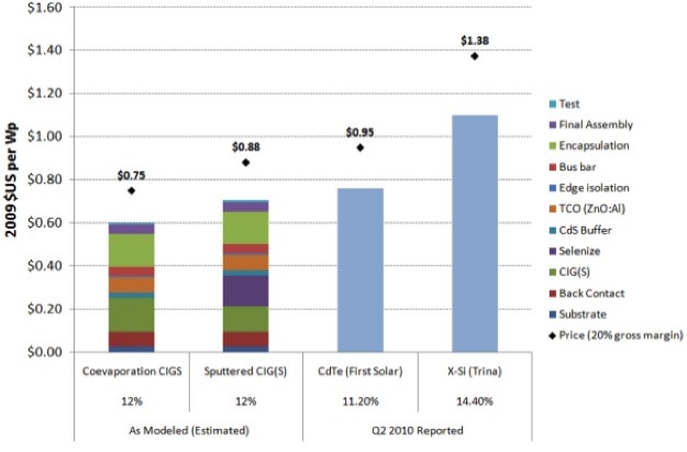 |
| Solar PV module manufacturing costs, benchmarking analysis: CIGS vs. CdTe and x-Si incumbents. Module costs must be considered in the context of module efficiency, i.e. impact on installation costs. |
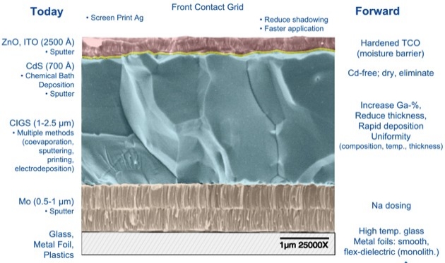 |
| Device structure varies between monolithically and mechanically integrated modules. (Source: NREL) |
The adjacencies session then moved into LEDs, with David Bour, chief technologist for LED product technology at Applied Materials, speaking on epitaxial nitride semiconductors for solid-state lighting. Light extraction is improved by using a patterned sapphire substrate that encourages defect pinning. A white light is fabricated by combining a blue LED with yellow phosphors to approximate the whiteness equivalent of black body radiation at ~4200°K. Visual repeatability is heavily dependent on thickness and composition uniformity in each layer; this is difficult, so device binning is used to approximate visual uniformity in the end package. Preliminary data indicates that the junction quality of the AMAT 450nm devices is superior to that of commercial 475nm devices, based on the observed absence of nonradiative defects at low currents. These devices were fabricated to demonstrate the benefits of run-to-run reproducibility in automated multilayer MOCVD, and do not signal a move by AMAT into LED manufacturing.
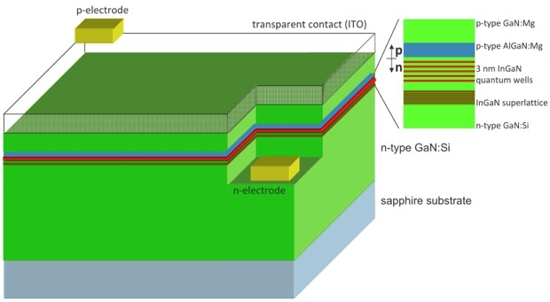 |
| LED epitaxial layer structure. |
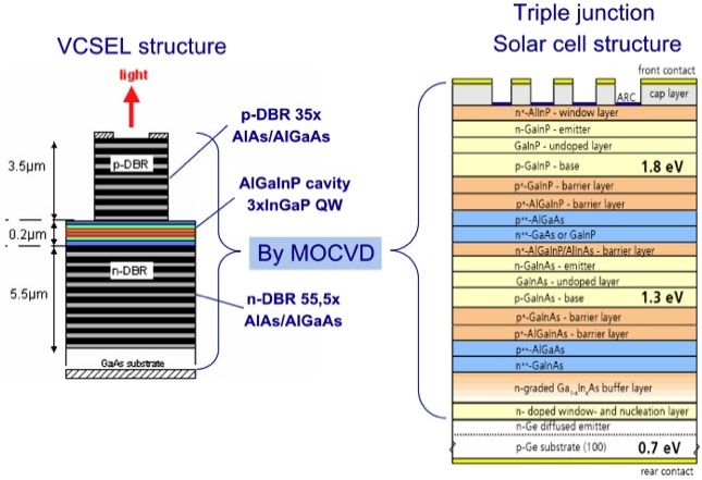
The final talk of the adjacencies session was on the MOCVD of III/V semiconductor by Johannes Kaeppeler, VP of technology at Aixtron. [Side note: Aixtron offers a PECVD carbon nanotube deposition tool called "Black Magic"; I like the way these guys think!] Aixtron’s revenue picked up sharply starting in 2007 due 90% to LEDs and the HDTV market, to the extent that they are already a $1B equipment company. I am personally fascinated by the complexity of multilayer structures that are already in volume production. The company’s long-term strategy calls for moving beyond LED and PV planar structures into CMOS III/V on Si, ready for production on 300mm & 450mm wafers in 3-4 years.
 |
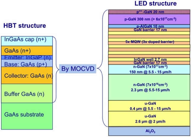 |
| Typical grown MOCVD structures. |
 |
| Integration of Ge p-channel and III-V n-channel using MOCVD. (Source: www.ims.demokritos.gr/DUALLOGIC/) |
Panel: Supply chain and materials
The traditional panel discussion on supply chain analysis and the materials business environment was moderated by Carl Johnson of Infrastructure, and began with a brief presentation by each of the five panelists.
- Tim Hendry, Intel VP and now head of its Fab Materials Organization, suggested some notions of improving materials affordability with supply chain innovation. Conflict-free minerals have moved very quickly from a level of social concern to government regulation, requiring rapid response by our industry.
- Norm Armour, VP/GM of GlobalFoundries Fab 8 in NY, is concerned about the materials cost escalation that accompanies design and device complexity. From 40nm to 28nm, materials costs are expected to double, while equipment costs will only increase 1.57times;. Immersion resist costs are 3-4× higher than DUV resist. Stronger lobbying is likely needed to protect the industry and specifically US interests.
- Roger Gossett, senior procurement manager at Freescale, dwelled on assurance of supply as a basic mantra, which resurrects the discussion of dual sourcing strategies and zero defects (although six sigma was never mentioned…).
- Jeremy How, strategic sourcing manager at Air Products, mapped out the intersection — collision, really — of volatility and complexity, and laid claim to having captured all of the points made by the prior three IDM speakers in his one chart. I do believe he may have done just that.
- Kurt Carlsen, strategic sourcing director for Air Liquide, monitors ISM data for US manufacturing looking for implications that will impact semiconductor supply chains from not-necessarily-expected sources. Those supply chains are now longer, more complicated, work on lower inventories, and require higher risks. He sees more of his suppliers planning to exit the semiconductor industry because many other industries provide greater stability in exchange for higher returns.
Johnson opened the panel discussion with a series of quick questions for individual panelists. Gossett is dealing with the huge bounce back in the automotive industry. Armour is spending capital at a rapid rate without necessarily being guaranteed of the material volumes needed to operate them. Hendry is running an abundance of tool qualifications while dealing with a too-high number of single source suppliers. How asserted that they can identify new suppliers for demand bubbles much more quickly than fab customers can qualify them. Carlsen expounded on the differences between procurement (day to day, price dominates) and sourcing (strategic, longevity dominates). Continually driving prices down ultimately results in suppliers exiting the business.
Raw material price increases drive delivered product prices (e.g. W powder needed for WF6), and this requires supplier-customer discussion, particularly in anticipation of expectations of price decreases if/when raw material prices decrease.
Electronic materials suppliers that simply repackage or ship direct from qualified sub-manufacturers are not often cut out as the middle man because they do provide a level of logistics management that fabs do not wish to replicate.
Hazardous materials shipped by boat can be refused loading by the captain, delaying the shipment until a captain comes along who is willing to convey the materials. Local manufacturing is the only solution to this problem for materials that cannot be shipped by air — of which the semiconductor industry uses several.
There is some marginal improvement in the US recently with manufacturing tax credits that make it possible to better maintain or upgrade US chemical manufacturing plants to keep the US competitive with emerging markets in China and elsewhere.
Michael A. Fury, Ph.D, is senior technology analyst at Techcet Group, LLC, P.O. Box 29, Del Mar, CA 92014; e-mail [email protected].

