January 12, 2011 — Popular consumer products such as smartphones, tablet PCs, and LED televisions have created demand for a new breed of low-cost advanced packaging technologies. There are a few key attributes in the highest demand for devices targeting these applications: a reduced footprint and/or profile, high electrical performance, fine-pitch design, custom features, and a low cost.
As consumer applications evolve into smaller, feature-rich devices, the supply chain must respond to meet these low-footprint, high-density component packaging demands. Over the last several years, the quad flat package no leads (QFN) package has been the standard device due to the benefits it offers (small, light, better thermal, etc.). Devices are getting smaller and are proving to be a challenge to assemble with finer pitches and longer bond wires. The introduction of dual-row QFNs has helped to reduce the package size and improved manufacturability. But these multi-row QFNs present their own challenges including finding manufacturers that can produce good lead features and ensuring the capability of an SMT house to mount multi-row QFN with no lead standoff height. In some cases, they also affect singulation by requiring a dual-pass process.
Newer technologies have taken the dual-row QFN a step further. The etched leadless package (ELP) offers flexibility with up to 3 rows with isolated pads, power and ground rings. This gives the device manufacturer options to optimize product performance. The triple-row capability provides an even smaller footprint having more I/Os. Another advantage of this package over standard QFNs is that the sawing process only cuts the mold compound, improving the cutting speed by >2× and extending saw blade life of the saw blade.
 |
 |
 |
 |
 |
| Figure 1. Variations of the etched leadless package (ELP). | ||||
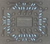
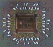
Another newer multi-row QFN-style package is QPL’s HDL technology. Unisem has collaborated with QPL to introduce the technology to their package portfolio in 2010 as their leadframe grid array (LFGA) package. The LFGA is similar to the ELP package — greater flexibility in a leadframe-based package — and allows for even greater customization to simplify the wire layout. The higher density routing also enables use of even more rows of leads to further reduce package size. Active leads can be placed underneath the die, attached by non-conductive epoxy or die attach film (DAF).
| 52 lead – 4.5x7mm form factor | 52 lead – 4×4.5mm form factor | ||
| Leadframe internal design | 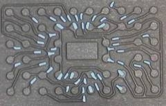 |
 |
|
| Front of line (FOL) assembly wire bonded | 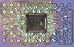 |
 |
|
| End of line (EOL) assembly after etching | 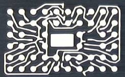 |
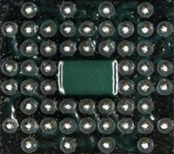 |
|
| Final package solder finish | 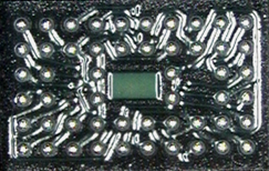 |
 |
|
|
Figure 2. Leadframe grid array package (LFGA). |
|||
For an even smaller package size, there has been strong surge in the demand of wafer level chip scale packaging (WLCSP). With features like its small footprint, thin profile, light weight, and cost competitiveness, it is a true chip-sized package where I/Os can be fully populated within the chip using a redistribution layer (RDL). Typical chips size range from about 1 × 1mm to 6 × 6mm with bump pitches of 0.4mm or larger. The WLCSP is utilized heavily in handheld products such as smartphones, tablet PCs, and digital still cameras.
Electrical performance continues to be a priority for packaging as well and is a requirement for most levels of devices in consumer electronics. The conventional wire bonded device has some limitations on when it comes to clock speed and cross-talk due to wire proximity. Using flip-chip technology improves the device response by >10% and at the same time gives better thermal performance 10~20% with the use of thermal bumps when attached to the thermal pad. Flip chip with Cu pillar bump technology can further help to improve the electrical performance. The WLCSP package technologies with direct ball drop on the pads or on redistributed pads will also have lower inductance when compared with standard wire bond.
Today’s complex devices also require fine-pitch design feature capabilities. Multi-row and fully populated QFN-style package offer design capabilities that in the past were limited to more expensive ball grid array (BGA) substrate-based packages. The previously mentioned packaging technology from QPL that Unisem has introduced as the LFGA is able to support 0.4mm pad pitch. Flip chip and WLCSP packages are also able to offer finer pitch features. Flip chip bumping technologies such as the Cu pillar bump can achieve a bump pitch of 120µm vs. electroplated solder bump (150µm) and conventional ball drop (400µm).
Custom packaging or even die-level features may also be required to meet today’s consumer electronic requirements. Multi-chip packages (MCMs), also known as system in package (SiP), integrate multiple chips and passive components within the package and help to reduce footprint, improving electrical performance and cost competitiveness. SiP is widely used in RF application products such as frontend power amplifier (PA) modules. Using an integrated passive device (IPD) to replace passive components in a SiP package is also gaining popularity. IPDs help to simplify the substrate and leadframe design for module packages, reducing the footprint and packaging lead time.
Conclusion
With all these needed features and advances in leadframe and flip-chip-based packaging solutions, the pressure is still on the assembly provider to offer all this at a competitive price. Leadframe-based packaging is generally more cost efficient than those that use substrates. QFN, multi-row QFN, ELP, LFGA, and other similar technologies have the ability to achieve higher I/Os and are very cost efficient. WLSCP packages using the ball drop process on 200 and 300mm wafer sizes is cost efficient because there are no direct packaging materials required and it simplifies the back-end assembly processes.
Other assembly process solutions that can help lower the assembly cost are Cu wire bonding, smaller wire diameter, lower-cost bill of materials (BOMs), post wire bond taping, and using a jig saw instead of tape saw for QFN. Pre-plated leadframes (PPF) can also lower the cost of the assembly processes.
Leadframe and flip-chip packaging technologies continue to evolve and help provide the semiconductor industry with package solutions that are both cost effective and able to take on the complexities of today’s and tomorrow’s consumer electronics market segment. Characteristics such as a reduced footprint and/or profile, electrical performance, fine pitch design, custom features and a low cost are now able to be achieved with technologies such as the ELP multi-row QFN package and with bumping technologies such as the fine pitch copper pillar bump. Device manufacturers no longer need to migrate to BGA-style packaging when requirements become demanding or complex.
Rico San Antonio of Unisem (Batam, Indonesia) co-authored this article with Chris Stai, Unisem (Sunnyvale, CA). Contact them at [email protected].
Subscribe to Solid State Technology/Advanced Packaging.
Follow Advanced Packaging on Twitter.com by clicking www.twitter.com/advpackaging. Or join our Facebook group

