By Debra Vogler, senior technical editor
February 7, 2011 — Researchers at imec — Danae Delbeke, photonics technology developer, INTEC (imec’s associated laboratory at Ghent U.) and Francesco Pessolano, manager, NVISION Program, imec — discuss announcements made in conjunction with Photonics West (January 25-27, 2011, San Francisco, CA) regarding the research consortium’s NVISION program (for advanced imaging solutions) and silicon.
Listen to the interviews here: Download (iPhone/iPod users) or Play Now
Pessolano describes the NVISION Program (announced 6 months ago) and explains in detail some of the changes that had to be made to standard CMOS processing to accommodate the requirements for hyperspectral imaging and smart lenses. For example, imec uses the Fabry-Perot effect instead of the complex optics (i.e., splitting light using prisms) used in conventional hyperspectral imaging; the result is a more cost-effective solution that is easily integrated. Pessolano said that the new imaging solution is 100× cheaper and 10-60× faster than the conventional imaging system.
 |
 |
|
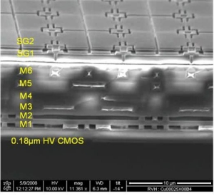
Figure 1. Cross-sectional view of integrated micro-mirror array, showing the mirrors (SG1 electrode and SG2 structural layer) on top fo the 6 layers (M1-M6) of Al interconnect. SOURCE: imec |
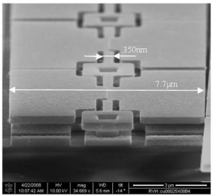
Figure 2. Top view of individual mirror, size 7.7µm, spacing 300nm, hinge width 350nm, phase step in center. SOURCE: imec |
Imec’s MEMS-based solution for smart lenses (two mirrors that deform to accomplish the zoom function) uses micro-mirrors (Figs. 1, 2). Pessolano discusses why it is necessary to control the tilt angles in an "analog" manner rather than digital. He also explains the materials selection and other factors (such as fill factor, and space constraints) important to the solution. The changes required a complete redesign of the micro-mirror topology, taking about 18 months for the redesigned MEMS-based device.
 |
 |
|
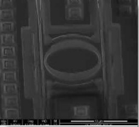
Figure 3. Advanced passive silicon photonics processes. SOURCE: imec |
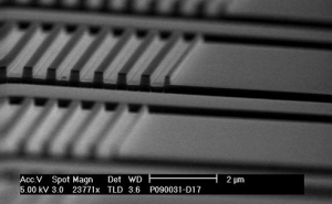
Figure 4. Highly efficient grating couplers realized by amorphous silicon deposition. |
Imec’s silicon photonics platform allows for the miniaturization of complex photonic functions on a single chip, i.e., a dense integration of photonics and electronics (Figs. 3, 4). Delbeke observes that reusing the wafer scale processes for silicon photonics, especially if the volumes are high, is cost-effective. Imec has also been standardizing the main optical building blocks for additional cost efficiency.
Follow Small Times on Twitter.com by clicking www.twitter.com/smalltimes. Or join our Facebook group

