|
Executive Overview This paper will discuss the use of projection lithography to improve overlay, print smaller minimum feature sizes without introducing defects, and address the need for improved resist profiles to deliver improved line width control for HBLEDs. The process performance that was achieved and consequent improvements enable higher device yields; higher yields directly impact device cost, resulting in accelerated adoption of this technology. |
Manish Ranjan, Doug Anberg, Warren Flack, Ultratech Inc., San Jose. CA USA
High-brightness light-emitting diodes (HBLED) can provide a substantial cost reduction for various niche lighting applications. It is anticipated that solid-state lighting will play a significant role in realizing global energy cost savings within the next several years. However, manufacturing cost reductions are critical to ensure wide spread adoption of LEDs for solid-state lighting. These manufacturing cost reductions are typically achieved via wafer size transitions, improved tool productivity and process yield improvements.
Lithography
Lithography is one of the key process steps affecting the final device and yield for high- brightness LED manufacturing. In general there are typically four to six lithography steps in a conventional LED manufacturing process and more may be added to increase the LED extraction efficiency. Many HBLED manufacturers currently use contact or proximity printers on 2-inch and 4-inch sapphire wafers. As the HBLED design rules are tightened to improve light extraction efficiency, contact and proximity aligners can become the limiting factor in HBLED yields due to high defect densities, line width control, and layer-to-layer overlay limitations.
Yields and manufacturing costs
Over the past 30 years, the semiconductor industry has achieved ~500x improvements in yielded silicon per unit time while continuously driving higher productivity of capital equipment. Semiconductor capital equipment today is more efficient, more productive, and less costly in terms of yielded silicon. Some of the cost-reductions for mature semiconductor manufacturing are summarized in Table 1 [1].
 |
|
Table 1. Estimated productivity improvements obtained by the semiconductor industry, resulting in ~500x more silicon per unit time yielded on today’s capital equipment tools when compared to tools in 1975. |
Similar manufacturing cost reductions are critical to the long-term success of the large-scale implementation of solid-state lighting (SSL). The LED industry needs to continue to implement processes to reduce costs or increase productivity in order to achieve the required cost targets for large-scale SSL implementation. A key contributor to the more advanced HBLED processes for SSL applications is the cost impact of the lithography process steps.
HBLED lithography. Many HBLED manufacturers that have historically utilized contact or proximity printers on 2-inch and 4-inch sapphire wafers are now transitioning to projection lithography. The use of projection lithography improves overlay, enables printing of much smaller minimum feature sizes without introducing defects, and provides superior resist profiles for improved linewidth control. The effect of these process improvements is higher device yield, which directly impacts device cost.
Contact and proximity printing. Contact and proximity printers image the wafer by using a full wafer sized mask that places the mask in contact or close proximity to the wafer and the shadow of the mask defines the structure on the exposed wafer. For an aligner, the optimum exposure condition for the mask to wafer working gap setting is often a difficult compromise between near contact for best image quality and a large gap space to minimize mask and resist damage due to mask to wafer contact. Because the minimum resolution required for today’s HBLED processes can be 5µm or less, the aligner gap is typically set to ~10µm or less.
2-inch sapphire substrates can have up to 50µm or more of bow as a result of the MOCVD process used in HBLED manufacturing, while 4-inch substrates have been shown to exceed 100µm of bow [2]. As a result, the mask will contact the substrate at various locations across the wafer, producing localized defects on the substrate being exposed. Additional defects are also generated on subsequent substrates when resist sticks to the mask and scatters light on subsequent exposures or transfers resist to the next substrate The present solution used in LED manufacturing is to frequently clean the mask, and replace the mask after several lots have been processed. This procedure adds significant recurring mask cost and unpredictable yield loss due to mask-generated defects.
In addition, as LED manufacturers adopt larger wafer sizes the sapphire substrate warpage increases significantly. This makes critical dimension control more difficult for full wafer mask imaging, as there can be a larger variation in the mask to wafer gap on larger wafer sizes (ranging from hard contact to several microns across the wafer).
Projection lithography. In projection lithography, a stepper uses projection optics to image a mask onto the substrate. The mask and wafer are separated by the projection optics and never come into contact. For projection lithography, the depth-of-focus (DOF) scales with the minimum feature size and provides significant DOF for imaging the one micron and above geometries required for HBLED production.
Another important advantage of projection lithography steppers for HBLED processing is the ability to image on severely warped substrates. A projection system can re-focus from field to field, so the gap variations across the wafer can be eliminated. Because the mask is never placed in proximity to the substrates, defects are not generated and the mask is never replaced due to contact damage. The elimination of defects from the lithography step with projection lithography provides higher yields than with contact or proximity print lithography.
It is possible for a stepper to compensate for topology that will allow the stepper to properly expose patterns onto warped substrates. Topology compensation can be accomplished by first mapping out the warpage profile of the wafer and locating the alignment features associated with each die. By adjusting the wafer tilt and the focus of the system, it is possible to align properly and to expose features. As warpage increases with larger wafer sizes, the ability of the lithography tool to compensate for substrate warpage becomes even more critical. Mask-to-wafer contact using aligners can occur over a larger area on the larger substrate, resulting in greater yield loss due to mask contact induced defects [1].
Process performance
1X projection steppers, which use projection lithography, can provide production process resolution down to 0.8µm, and have the capability to meet future potential sub-micron HBLED lithography requirements for enhanced light extraction process steps [3]. This represents a greater than 5x improvement in the practical production resolution limit of ~5µm for aligners due to defect and line width control limitations.
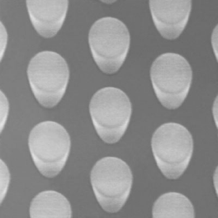
Two lithography steps clearly demonstrate the resolution advantages of projection lithography. The first is a patterned sapphire substrate (PSS) step that acts as a reflector under the LED to increase the light extraction efficiency. In addition to enhancing light extraction efficiency, PSS structures can also help reduce the dislocation defect density, which helps in improving the overall device efficiency. The PSS consists of a repeating grid structure that is etched into the sapphire to scatter light. The efficiency of the PSS increases as the size of the grid structure is reduced to 1µm features (Fig. 1) [4]. The uniformity of size of the structure and consistency of the resist profile of the PSS pattern is important to obtain maximum efficiency for the reflector.
 |
|
Figure 1. PSS layer with 1µm pillars and spaces in a 3µm thick photoresist. |
The second lithography step is a current spreading layer that is used to enhance the brightness of the LED. The current spreading features have small widths to maximize the current injection area across the device while minimizing the area of the LED that is blocked by the current spreading structures [4].
 |
|
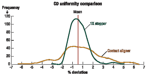
Figure 2. The CD uniformity from a 1X stepper is superior to a contact aligner. These results were from a 10µm pattern on a silicon wafer. |
Projection lithography also provides better critical dimension (CD) control than a wafer aligner. End user experimental data comparing the CD uniformity for large 10µm features on Si wafers showed 2% variation for the 1X stepper and 6% for the wafer aligner as shown in Fig. 2 [5].
The stepper provides more uniform and reproducible linewidths, which result in higher yields. For sapphire substrates used for LED fabrication, wafer warpage can lead to variations in line width that are much greater than when using a wafer aligner on silicon wafers because the substrates are rigid and typically highly warped. In the case of a stepper with a projection lens, the line width variation on the sapphire substrates will be minimal due to the ability to independently focus every exposure step.
Projection lithography provides better layer-to-layer overlay than a full wafer aligner. End user experimental data comparing product overlay on silicon wafers showed 3-sigma overlay better than 0.4µm for a 1X stepper vs. 2.0µm for the full wafer aligner. Because each field is independently exposed and aligned, a stepper can correct for many systematic wafer scale errors such as grid and orthogonality during the step and repeat exposure process. This stepper capability results in superior layer to layer overlay compared to the full-wafer exposures required with contact and proximity aligners.
Conclusion
The move towards clean renewable energy sources along with broad government incentives is driving the adoption of LED technology for the general lighting market segment. Significant improvements in manufacturing processes and infrastructure development are critical to ensure overall adoption of LEDs. Lithography is one of the critical processes affecting overall device yield and performance. The use of 1X steppers provides significantly better technology and economic advantages for high-volume manufacturing environments.
References
1. D. Anberg, A. Hawryluk, "Low Cost of Ownership Lithography for High Brightness LED Manufacturing," LED Prof. Review, Nov/Dec 2009.
2. E. Armour, F. Lu, M. Belousov, D. Lee, W. Quinn, "Semiconductor Today, Compounds and Advanced Silicon," Vol. 4, Issue 3, April/May 2009.
3. G. Flores, L. Dwyer, W. Flack, "Lithographic Performance of a New Generation i-line Optical System," SPIE 1927, 1993 Proc.
4. E. Schubert, Light-Emitting Diodes, Cambridge U. Press, 2007.
5. D. Anberg, M. Eguchi, T. Momobayashi, T. Wakabayashi, T. Miyamoto, "1X Broadband Wafer Stepper for Bump and Wafer Level Chip Scale," Packaging (CSP) Applications, Pan Pacific 2000.
Biographies
Manish Ranjan received his MBA from The Wharton School of Business and MS from State U. of New York and is VP, Advanced Packaging and Nanotechnology Markets at Ultratech, Inc., 3050 Zanker Road, San Jose, CA 95124 USA; ph.: (800) 222-1213; email [email protected]
Doug Anberg received his BS degrees in chemistry and electronic engineering from California Polytechnic State U. and a masters in engineering management from Santa Clara U. and is VP, Advanced Stepper Technology, at Ultratech, Inc.
Warren Flack received his BS and MS in chemical engineering from the Georgia Institute of Technology and his PhD in chemical engineering from the U. of California, Berkeley. Warren. is Senior Director of Worldwide Applications at Ultratech, Inc.
More Solid State Technology Current Issue Articles
More Solid State Technology Archives Issue Articles

