By Debra Vogler, senior technical editor
March 11, 2011 — Among the topics covered at KLA-Tencor’s annual Lithography Users Forum (2/27/11) at the SPIE Advanced Lithography Conference (2/27-3/3/11) was extension of KLAC’s Teron 600 platform for inspection of EUV blanks at the 16nm half pitch (hp) node.
 |
|
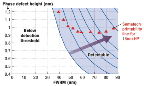
Figure. Blank inspection: Teron platform extension defect signal sufficient for 16nm HP (1 × 50nm FWHM). |
When KLAC released the Teron 600 inspection system, the impetus was industry’s need to simultaneously evaluate several lithography technologies for use at the 2Xnm, including spacer pitch splitting/pattern cutting, true pitch splitting, inverse lithography/source mask optimization, as well as EUV. The figure shows simulation results from the 600 platform for inspection of EUV blanks at the 16nm hp node.
Listen to Trafas’ interview: Download (iPod/iPhone users) or Play Now
In a podcast interview recorded at the event, Brian Trafas, chief marketing officer at KLA-Tencor, discusses the process control needs facing the semiconductor industry, including cost of ownership (COO) and key metrology parameters for 193nm lithography, such as overlay control. One EUV-specific challenge is achieving defect-free masks. To that end, the company has been working on infrastructure needed for mask monitoring (reticle inspection for blanks and patterned masks), as well as patterned wafer defect solutions.
Subscribe to Solid State Technology/Advanced Packaging.
Follow Solid State Technology on Twitter.com via editors Pete Singer, twitter.com/PetesTweetsPW and Debra Vogler, twitter.com/dvogler_PV_semi.

