3D-CT-X-ray-imaging-fills-inspection-gaps-says-Xradia

By Debra Vogler, senior technical editor

March 29, 2011 — Xradia has unveiled its latest micro computed tomography (CT) 3D X-ray imaging system, the VersaXRM, targeting gaps in the semiconductor, materials science, geomaterials, and life sciences market segments. Kevin Fahey, PhD, VP of marketing at Xradia, told ElectroIQ that the new system is able to provide a large working distance (i.e., the distance between the source spot and rotation axis of the sample) at high resolution (non-destructive).
Click to Enlarge
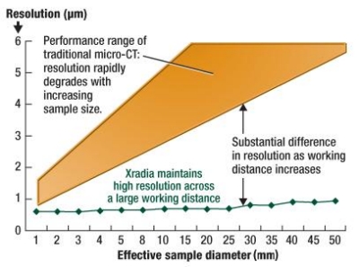
Figure 1. Maintaining resolution across a large working distance. Source: Xradia.

Xradia says that the system can handle a >10× larger sample size for imaging at the same resolution as conventional systems. Large working distances are important to these market segments as they enable in-situ study using environmental chambers or load cells as well as study under varying environmental conditions.

Complex 3D packaging has generated an additional class of defects that come about because of the new solder and dielectric materials, and geometries (e.g., sub-micron voids and cracks). These defects are difficult to detect inside an intact package.

Listen to Fahey’s interview: Download (iPod/iPhone users) or Play Now

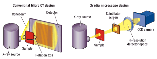
In this podcast interview, Fahey discusses how the new platform uses geometrical magnification in tandem with an X-ray microscope. Conventional microCT systems use only geometric magnification technology. By coupling geometrical magnification and optical magnification, "the combination gives very high resolution and allows the sample to sit in an environment where it is not overly sensitive to position away from the source, so we can use larger samples, or larger source-to-sample distances while maintaining high resolution," said Fahey. Modest geometrical magnification (small cone angle) works in tandem with high optical magnification.
Click to Enlarge
Figure 2. Resolution working distance benefits of microscope design. Source: Xradia.

There are many different elements that contribute to resolution: a combination of spot size of the source, the geometry of the system, the resolution of the camera, the scintillator material, vibrations in the system, any thermal variance, and so forth. "Because it’s difficult to test and specify resolution, it’s common place to focus on one of these elements as the dominant factor," noted Fahey. Conventional geometric projection systems tend to be overly sensitive to spot size, called spot blurring (fringes around the sample), explained Fahey. In comparison, the new system is not sensitive to spot size, which means larger spot sizes can be used. In turn, this means larger sources, which are inherently more stable, can be used, improving reliability.  
Click to Enlarge

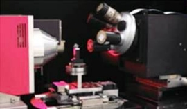
Figure 3. Xradia microscope.

Fahey concludes the interview discussing throughput of a typical 3D IC package failure analysis.

Subscribe to Solid State Technology/Advanced Packaging.

Follow Solid State Technology on Twitter.com via editors Pete Singer, twitter.com/PetesTweetsPW and Debra Vogler, twitter.com/dvogler_PV_semi.

Or join our Facebook group

POST A COMMENT

Easily post a comment below using your Linkedin, Twitter, Google or Facebook account. Comments won't automatically be posted to your social media accounts unless you select to share.

3D CT X ray imaging fills inspection gaps says Xradia

By Debra Vogler, senior technical editor

March 29, 2011 — Xradia has unveiled its latest micro computed tomography (CT) 3D X-ray imaging system, the VersaXRM, targeting gaps in the semiconductor, materials science, geomaterials, and life sciences market segments. Kevin Fahey, PhD, VP of marketing at Xradia, told ElectroIQ that the new system is able to provide a large working distance (i.e., the distance between the source spot and rotation axis of the sample) at high resolution (non-destructive).

Click to Enlarge
Figure 1. Maintaining resolution across a large working distance. Source: Xradia.

Xradia says that the system can handle a >10× larger sample size for imaging at the same resolution as conventional systems. Large working distances are important to these market segments as they enable in-situ study using environmental chambers or load cells as well as study under varying environmental conditions.

Complex 3D packaging has generated an additional class of defects that come about because of the new solder and dielectric materials, and geometries (e.g., sub-micron voids and cracks). These defects are difficult to detect inside an intact package.

Listen to Fahey’s interview: Download (iPod/iPhone users) or Play Now

In this podcast interview, Fahey discusses how the new platform uses geometrical magnification in tandem with an X-ray microscope. Conventional microCT systems use only geometric magnification technology. By coupling geometrical magnification and optical magnification, "the combination gives very high resolution and allows the sample to sit in an environment where it is not overly sensitive to position away from the source, so we can use larger samples, or larger source-to-sample distances while maintaining high resolution," said Fahey. Modest geometrical magnification (small cone angle) works in tandem with high optical magnification.

Click to Enlarge
Figure 2. Resolution working distance benefits of microscope design. Source: Xradia.

There are many different elements that contribute to resolution: a combination of spot size of the source, the geometry of the system, the resolution of the camera, the scintillator material, vibrations in the system, any thermal variance, and so forth. "Because it’s difficult to test and specify resolution, it’s common place to focus on one of these elements as the dominant factor," noted Fahey. Conventional geometric projection systems tend to be overly sensitive to spot size, called spot blurring (fringes around the sample), explained Fahey. In comparison, the new system is not sensitive to spot size, which means larger spot sizes can be used. In turn, this means larger sources, which are inherently more stable, can be used, improving reliability.  

Click to Enlarge

Figure 3. Xradia microscope.

Fahey concludes the interview discussing throughput of a typical 3D IC package failure analysis.

Subscribe to Solid State Technology/Advanced Packaging.

Follow Solid State Technology on Twitter.com via editors Pete Singer, twitter.com/PetesTweetsPW and Debra Vogler, twitter.com/dvogler_PV_semi.

Or join our Facebook group

POST A COMMENT

Easily post a comment below using your Linkedin, Twitter, Google or Facebook account. Comments won't automatically be posted to your social media accounts unless you select to share.