By Debra Vogler, senior technical editor
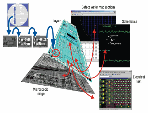
March 8, 2011 — During the SPIE Advanced Lithography Conference (2/27-3/3/11, San Jose, CA), Applied Materials (AMAT) and Magma Design Automation announced that Magma’s CAD-based navigation and yield analysis software has been integrated with Applied Materials’ inspection systems; it’s called Excalibur Litho (see figure) and targets designs at 2xnm and below. The companies claim that, without the ability to overcome litho qualification roadblocks rapidly, 22nm designs will be extremely time-consuming and expensive to bring to volume production.
 |
| Figure: Excalibur Litho enables litho defects to be cross-mapped to layout, netlist, schematic, and electrical test. SOURCE: Magma/Applied Materials (AMAT). |
By combining inspection and yield analysis, the companies aim to accelerate lithography qualification and improve chip yield at advanced nodes. The companies believe the system will be forward-compatible with extreme ultraviolet (EUV) lithography. Complex interactions between process conditions and design produces hot spots (areas where the printed pattern deviates from the design intent) that stall a chip’s move to production. Integrating design and real-time inspection data identifies hot spots in a production environment and the conditions that produce hot spots can be fed back to the design process. Erez Paran, integrated solutions manager, Process Diagnostics & Control, Applied Materials, said that being able to clear hot spots left over from simulation will enable faster time to market with higher yield for end users’ products.
Listen to the interviews: Download (iPhone/iPod) or Play Now
Ankush Oberai, GM & VP, Fab Analysis Business Unit at Magma Design Automation, explained that in-line information from inspection review systems can be used to do correlation with the design, instead of pre-tape-out. Given shrinking geometries — particularly below 20nm — actual data (from inspection review systems) is necessitated to be correlated to form a library. "We’re bringing data from all aspects of design, i.e., layout, netlist, schematic, simulation, and electrical test, as well as diagnostic information," said Oberai. The data is correlated to a specific defect spot that can then be identified and compared to incoming data, he said.
Subscribe to Solid State Technology/Advanced Packaging.
Follow Solid State Technology on Twitter.com via editors Pete Singer, twitter.com/PetesTweetsPW and Debra Vogler, twitter.com/dvogler_PV_semi.

