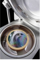
March 17, 2011 — Applied Materials Inc. (AMAT) introduced the Applied Centura Conforma, with conformal plasma doping (CPD) targeted for 22nm and beyond logic and memory chips. The technology replaces ion beam implantation for conformal doping of complex 3D structures.
 The Conforma system combines high-dose, low-energy doping technology with in-situ clean capability in a single vacuum chamber to deliver uniform, high throughput doping on both planar and 3D structures. The system uses a pure, additive-free doping chemistry that preserves the underlying device structures.
The plasma doping technology draws from AMAT technologies for RF engineering and CVD chamber design, said Sundar Ramamurthy, vice president and general manager of the Front End Products business unit at Applied Materials, adding that Conforma systems are running in customers’ pilot and high-volume manufacturing. "We’re also working with customers and research entities on pioneering R&D programs using our proprietary technology."
Doping is traditionally performed by bombarding the wafer with a beam of dopant ions moving at high speed. However, this straight line bombardment process cannot provide uniform doping of advanced three-dimensional structures. More importantly, the fast-moving ions can damage the ultra-thin semiconductor layers in cutting-edge chips. Applied’s Conforma technology provides a gentle, low-energy process that enables uniform, conformal doping over complex 3D chip structures. The Centura Conforma combines integrated plasma pre-clean and RTP anneal on the same vacuum platform.
Some of the advanced devices enabled by the new Conforma system include finFET logic, vertical gate DRAM and vertical NAND flash memory arrays.
Applied Materials, Inc. (Nasdaq:AMAT) provides equipment, services and software to enable the manufacture of advanced semiconductor, flat panel display and solar photovoltaic products. Learn more at www.appliedmaterials.com.
Subscribe to Solid State Technology/Advanced Packaging.
Follow Solid State Technology on Twitter.com via editors Pete Singer, twitter.com/PetesTweetsPW and Debra Vogler, twitter.com/dvogler_PV_semi.

