By Debra Vogler, senior technical editor
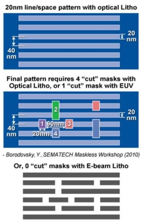
March 9, 2011 — At SPIE Advanced Lithography (2/27-3/3/11, San Jose, CA), David Lam, chairman of Multibeam Corp., and the founder and former CEO of Lam Research, presented the concept of complementary e-beam lithography (CEBL) — a technology that is being used to complement and extend optical lithography for advanced logic ICs.
Listen to David Lam’s interview: Download (iPhone/iPod users) or Play Now
In the podcast interview with Debra Vogler, senior technical editor, Lam discusses the technology in detail, and also cites the inspiration for his paper: a presentation on complementary lithography by Intel Senior Fellow Yan Borodovsky, at last year’s SPIE Advanced Lithography Conference. Also significant to CEBL is a presentation by Sam Sivakumar (Intel Fellow and director of lithography) at Nikon’s LithoVision event this year (2/27/11), in which he discussed how the layout design style of logic devices is migrating from 2D to 1D.
|
|
 |
Lam observes that IC manufacturers will find CEBL beneficial as they search for ways to continue using their optical lithography equipment — especially since so much of it is already amortized. It is anticipated that CEBL will be used in a mix/match manner with optical lithography for low-density critical layers (e.g., vias, line cuts, and contacts) in high-volume manufacturing.
More from SPIE Advanced Lithography 2011:
- AMAT inspection, Magma yield analysis integration to accelerate litho quals, better chip yields
- SPIE 2011: An ASML review of EUV
- SPIE: A glimpse into Intel’s litho future
- The physics behind Gigaphoton EUV source technology
- Cymer talks EUV source timelines and DUV highlights at SPIE
- EUV, resists, multibeam lithography chat with imec
- SPIE 2011: Where are we now with EUV?
- Carl Zeiss photomask registration correction system, RegC, debuts
- Cymer focus drilling for immersion light sources improves depth of focus by 2x
- Nanometrics launches overlay metrology system, wins order from Asia
- EUV lithography vs EBDW: Interview with Toppan Photomasks at SPIE
- Synopsys lithography verification in Proteus LRC handles EUV, double patterning
- SPIE keynote: Imec installs ASML pre-production EUV scanner NXE:3100
- Brewer Science launches immersion lithography products with OptiStack
Subscribe to Solid State Technology/Advanced Packaging.
Follow Solid State Technology on Twitter.com via editors Pete Singer, twitter.com/PetesTweetsPW and Debra Vogler, twitter.com/dvogler_PV_semi.


