Mirco Cantoro, imec, Leuven, Belgium
March 30, 2011 — Graphene has been widely hailed as replacement material for silicon. It does have remarkable characteristics that would allow it to take up that role. Today, the major hurdle that prevents its widespread use is technological: there are no reliable, large-scale techniques to produce and process graphene within the constraints of state-of-the-art semiconductor microfabrication. Therefore, given the current state-of-the-art of graphene technology, a fast replacement of the silicon-MOSFET with a graphene-based equivalent seems unrealistic. Graphene could find its place, however, in niche applications, such as in high-speed, high-frequency electronics, or alternatively in flexible, plastic electronics.
 |
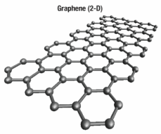
| Figure 1. Ball-and-stick model of the arrangement of carbon atoms in graphene, carbon nanotubes and fullerenes. The nanostructures share the same honeycomb lattice configuration, rolled up in different dimensions. |
Graphene, the thinnest material known in nature, is a 2-dimensional, atomically-thin sheet of carbon atoms arranged in a honeycomb lattice. It is also the basic building block of other carbon materials of different dimensionals, such as fullerenes, carbon nanotubes (CNT), and graphite (Fig. 1). Graphene was successfully isolated for the first time only in 2004 at the University of Manchester [1], although it had been the subject of theoretical studies for several decades before. This caused worldwide jaw-dropping among solid state physicists, because 2D crystals were not thought to exist. The discovery was followed by an exponentially growing number of publications on graphene. The two scientists who discovered graphene, A. Geim and K. Novoselov, were recently awarded the 2010 Nobel Prize in physics.
The main interest in graphene arises from the configuration of its energy band structure, making this material unique when compared to those employed in current semiconductor technology. Electrons in graphene behave as if they virtually possess no effective mass, and are therefore called Dirac fermions, a tribute to the Dirac equation describing the dynamics of massless particles. As a consequence, graphene possesses remarkable physical properties and exhibits “exotic” phenomena such as the fractional quantum Hall effect and Klein tunneling. Excellent current transport characteristics, unmatched optical performance, together with a strictly 2-dimensional character, are only a few of the features making graphene attractive for microelectronics.
Can we produce graphene for use in microelectronics?
So far, most of the experimental work performed on graphene is based on samples produced by micromechanical exfoliation, the technique that allowed its first successful isolation: it consists of peeling thin layers from graphite crystals, usually with the help of adhesive tape, and transferring them onto dielectric films for visual identification. Surprisingly, exfoliation provides samples of the best quality, used for most of the breakthroughs achieved in fundamental and applied research on graphene.
The drawback is that exfoliation is intrinsically not suitable for CMOS applications. The availability of a CMOS-compatible mass production technique will be a prerequisite to seriously consider graphene a valid alternative to silicon, stepping into the so-called "post-silicon era." Therefore, the challenge for graphene is in trying to develop a large-area deposition technique that would ensure a high quality material.
Promising results were obtained in graphene synthesis through annealing silicon carbide crystals, carried out at temperatures above 1300°C. Chemical vapor deposition of graphene on metal films at temperatures in the 800-1000°C range can also provide samples whose quality is second to that of exfoliated graphene. The latter approach could be improved by engineering the metal film used as support, so that the entire process flow becomes CMOS-compatible, from the material deposition to the device fabrication.
Main advantages of using graphene in CMOS
Carbon nanotubes share many properties with graphene that are advantageous for nanoelectronics. However, an obvious advantage of graphene is its 2-dimensional character, which enables straightforward CMOS processing. Planar microfabrication techniques, such as optical lithography and dry etching, can be transferred from the current silicon-based production technology to graphene without fundamental paradigm shifts. In fact, the advantage in using graphene would not only be limited to the gain in mobility over silicon, but also in the possibility to achieve extremely thin transistor channels that can maintain the current trend in CMOS scaling. Moreover, the 2-dimensional nature of graphene would be very helpful in providing a solution against short channel effects, allowing extreme scaling options. The intrinsic perfection of its lattice makes graphene very stable at nanometer sizes, even down to the single benzene ring; playing with graphene at these reduced sizes would present many similarities with molecular electronics. Perfect graphene channels would not exhibit performance fluctuations, such as those theoretically predicted for silicon and other semiconductors when squeezed to a few atoms across.
Charge carriers in graphene possess remarkably high mobilities, in excess of 104cm2V-1s-1 (measured for substrate-supported, exfoliated graphene), allowing for ballistic transport at lengths of several hundreds of nanometers at room temperature in pristine samples. The charge transport properties of graphene, together with the richness of the spin physics it exhibits, suggested the use of this material for the implementation of novel device concepts such as single-electron-, pseudospin-, or tunnel-effect-transistors.
Graphene obtained by wet chemical synthesis, such as reduced graphene oxide, could be the material of choice in low-cost applications. Its properties benchmark very well when compared with those of materials used today in plastic, flexible electronics. Liquid suspensions offer an inexpensive means to make graphene-based coatings by spin casting or printing techniques. These coatings could efficiently replace ordinary transparent conductors used in photovoltaic applications, thanks to their excellent optical properties.
Towards a graphene-based MOSFET
All MOSFETs fabricated with graphene as active channel exhibit extremely poor current modulation characteristics, due to the semi-metallic character of graphene. Even at zero applied gate voltage, at the point of minimum conductance (the so-called Dirac point), Ioff is large enough to render the transistor switch-off problematic. Also, the fabrication of top gates on graphene, and the interaction with supporting substrates in general, causes a decrease in the charge carrier mobility. In general, the presence of charge scattering centers, arising whenever graphene is placed in contact with another material, is detrimental for the performance of graphene devices. These factors represent another obstacle for a realistic replacement of silicon MOSFETs with graphene equivalents in logic applications.
Even with low Ion/Ioff, high-frequency applications of graphene could be realistic. Graphene has been predicted to achieve excellent performance even up to the THz range. Although the record performances of the state-of-the-art III-V devices are still unmatched, graphene equivalents show constant, steady progress in performance, indicating that they will close the gap soon.
The problem of the low Ion/Ioff could be solved by introducing a bandgap in graphene while retaining the superb transport characteristics. One of the solutions that has been proposed theoretically (and later verified experimentally) is to tailor graphene into ribbons, causing the opening of a quantum confinement-induced bandgap. There are at least two major fundamental problems with this approach: first, the ribbons would have to be fabricated with a precise, reproducible configuration of the edge atoms; second, as bandgap and mobility scale inversely with the ribbon width, reasonable bandgaps could be achieved only in ribbons a few nanometers wide. The reduced size would also cause the significant suppression of the device performance.
While electron-beam lithography can assist the research in graphene ribbon fabrication by providing flexibility in fast prototyping, a decisive effort would need to be provided by optical lithography. It represents the only commercially viable option today, and solutions for reproducible sub10nm planar patterning might be available soon. Additionally, unless a technique to achieve highly controlled, anisotropic planar etching for graphene is developed, one would have to deal with graphene ribbons having irregular edges, with a detrimental effect on both device performance and process reproducibility.
 |
|
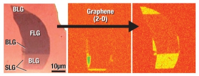
Figure 2. Optical microscopy image (left) of a graphene flake composed of single-layer (SLG), bi-layer (BLG) and few-layer parts (FLG). The sample is subjected to an oxygen plasma at progressively longer exposure times. Photoluminescence maps (center, right) show that the thinnest plasma-treated graphene regions become luminescent, indicating the opening of an optical bandgap in the material. |
Alternative approaches in building up a bandgap in graphene rely on the breaking of its symmetry by depositing graphene bilayers on suitable substrates, by applying transverse electric fields, or by decorating its surface with specific functional groups. The latest approach has been pursued at imec by carrying out a series of experiments in which graphene has been exposed to different plasma atmospheres; its optoelectronic performance results tunable and function of specific process parameters [2] (Fig. 2). This line of research is part of a larger, ambitious endeavor that sees imec involved in the search for a solution to the problem of manufacturability and integrability of graphene in conventional semiconductor process flows; more in general, the research at imec is about searching for the answer to the question of whether or not graphene will ever be a useful material in nanoelectronics.
Conclusion
Although a replacement of the silicon MOSFET with a graphene-based equivalent seems unrealistic, when looking at the current status of the related technology, graphene could find room in niche applications, such as in high-speed, high-frequency electronics. At the same time, graphene could easily fit in the growing trends ruling the market of flexible, plastic electronics. At the moment, technology, not physics, represents the major hurdle to allow graphene to step out of the lab and pave the way that leads to the future of technology, either alone, or hand-in-hand with silicon.
References
[1] K.S. Novoselov, A.K. Geim, S.V. Morozov, D. Jiang, Y. Zhang, S.V. Dubonos, Science 306, 666 (2004).
[2] A. Nourbakhsh, M. Cantoro, T. Vosch, G. Pourtois, F. Clemente, M. H. van der Veen, et al., Nanotechnology 21, 435203 (2010).
Mirco Cantoro received the Laurea degree in physics from the U. of Pisa (Italy) in 2001 and a PhD in electrical engineering from the U. of Cambridge (UK) in 2006. He is a senior research scientist at imec. Contact Cantoro at [email protected].
Follow Small Times on Twitter.com by clicking www.twitter.com/smalltimes. Or join our Facebook group

