March 4, 2011 — Researchers in the University of Arizona’s physics department, along with collaborators from the Massachusetts Institute of Technology (MIT) and the National Materials Science Institute in Japan, found that by placing a graphene layer on a material almost identical in structure, boron nitride (BN), instead of the commonly used silicon oxide (SiO2) found in microchips, they could significantly improve its electronic properties.
 |
|
Placed on boron nitride, graphene shows much smaller electric charge fluctuations, shown in red and blue (left) than when mounted on a silicon oxide wafer (right). (Image courtesy of Brian LeRoy/UA) |
The study of the physical properties and potential applications of graphene has suffered from a lack of suitable carrier materials that can support a flat graphene layer while not interfering with its electrical properties, the researchers said.
Substituting silicon wafers with boron nitride, a graphene-like structure consisting of boron and nitrogen atoms in place of the carbon atoms, the group was the first to measure the topography and electrical properties of the resulting smooth graphene layer with atomic resolution.
 |
|
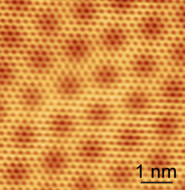
Under the scanning tunneling microscope, graphene reveals its honeycomb structure made up of rings of carbon atom, visible as small hexagons. The larger hexagons result from an interference process occurring between the graphene and the underlying boron nitride. The scale bar measures one nanometer, or one billionth of a meter. (Image courtesy of Brian LeRoy/UA) |
"Structurally, boron nitride is basically the same as graphene, but electronically, it’s completely different," said Brian LeRoy, an assistant professor of physics and senior author of the study. "Graphene is a conductor, boron nitride is an insulator."
"We want our graphene to sit on something insulating, because we are interested in studying the properties of the graphene alone. For example, if you want to measure its resistance, and you put it on metal, you’re just going to measure the resistance of the metal because it’s going to conduct better than the graphene."
To measure the topography of the graphene surface, the team uses a scanning tunneling microscope, which has an ultrafine tip that can be moved around. "We move the tip very close to the graphene, until electrons start tunneling to it," Jiamin Xue, a doctoral student in LeRoy’s lab and the paper’s leading author, explained. "That’s how we can see the surface. If there is a bump, the tip moves up a bit."
"Using a scanning tunneling microscope, we can look at atoms and study them," Leroy added. "When we put graphene on silicon oxide and look at the atoms, we see bumps that are about a nanometer in height. Boron nitride…smooths out the bumps by an order of magnitude."
For the spectroscopic measurement, Xue holds the tip at a fixed distance above the sample. He then changes the voltage and measures how much current flows as a function of that voltage and any given point across the sample. This allows him to map out different energy levels across the sample.
"You want as thin an insulator as possible," LeRoy added. "The initial idea was to pick something flat but insulating. Because boron nitride essentially has the same structure as graphene, you can peel it into layers in the same way. Therefore, we use a metal as a base, put a thin layer of boron nitride on it and then graphene on top."
"When you have graphene sitting on silicon oxide, there are trapped electric charges inside the silicon oxide in some places, and these induce some charge in the overlying graphene. You get quite a bit of variation in the density of electrons. If graphene sits on boron nitride, the variation is two orders of magnitude less," LeRoy said.
The team’s results are published in the advance online publication of Nature Materials.
 |
|
Jiamin Xue, Philippe Jacquod and Brian LeRoy (left to right) with the scanning tunneling microscope they use to study graphene. (Photo by Patrick McArdle/UANews) |
In addition to potential applications in integrated circuits, solar cells, miniaturized bio devices and gas molecule sensors, graphene has attracted the attention of physicists for its unique properties in conducting electricity on an atomic level. Graphene has little resistance and allows electrons to behave as massless particles like photons while traveling through the hexagonal grid at very high speeds.
The UA portion of this research was funded by the U.S. Army Research Office and the National Science Foundation.
Follow Small Times on Twitter.com by clicking www.twitter.com/smalltimes. Or join our Facebook group

