John Robinson, director of marketing, Process Control Information Division (PCID), KLA-Tencor (KLAC)
March 30, 2011 — In-line automated inspection during wafer fabrication allows high defect capture rates (consistency, accuracy) and rapid classification (time-to-results) of mission-critical defects. However, to achieve the most value from a comprehensive automated inspection investment, advanced defect analysis is needed. Incorporating defect data from multiple inspections throughout the LED manufacturing process into one environment provides a holistic approach, as well as unprecedented process control and yield improvement.
Many LED fabs currently have only basic manual methods to perform defect and yield analysis. The bulk of engineering time is spent gathering and formatting, slowing time to results. Too often, methods are inconsistent, without advanced analysis tools, and lack connectivity between process areas, such as incoming bare wafer inspection, epi inspection, patterned wafer inspection, post dice inspection, and final electrical yield probe inspection.
A better approach includes a centralized database capable of handling inspection data and images, metrology data, yield bin data, as well as fab process inputs. Combined with advanced analysis tools and automation, engineers can quickly and effectively get results.
 |
|
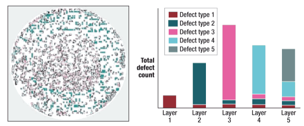
Figure. Advanced defect source analysis (DSA). KLARITY LED provides defect source analysis including interactive wafer maps and images. |
Defect source analysis (DSA) (see figure) includes both qualitative and quantitative methods to determine where in the process defects are introduced, which defects are common from one process step to the next, and how the defects propagate throughout the production line. Knowing, for example, that defects found post-dice originated back in the epi process will save valuable time identifying the root cause and will reduce the amount of material at risk.
Spatial signature analysis (SSA) enables automated detection of defect signatures, such as scratches or other characteristic spatial patterns. Frequently, simple statistical process control (SPC) on overall defect counts is insufficient to detect problems with unique assignable causes that can readily be identified with SSA. For example, an intermittent resist spin-on issue may appear to be a random scratch. Identified by SSA and viewed as an aggregate over many wafers, however, the tell-tale wagon-wheel pattern can be readily identified.
The LED industry is beginning to adopt stepper-based projection lithography. This introduces an additional class of defects, called repeating defects to distinguish them from random defects. Defects introduced as part of stepper-based lithography can repeat from projection field to projection field many times across an individual wafer, as well as from wafer to wafer. Repeater defect analysis tools can quickly determine if the lithographic process is drifting out of spec and save many die that would otherwise fail as non-yielding die.
A defect early in the manufacturing process wastes not only the costs related to the defective wafer itself, but also any additional processing of the defective wafer, and the costs of any additional wafers that suffer yield loss before the excursion is identified. By inserting in-line inspection points at significant process milestones, as well as adopting advanced defect analysis solutions, manufacturers can catch excursions sooner, reducing the amount of product at risk.
Minor excursions are due to a shift in process parameters that is not significant enough to trigger an alarm using only basic SPC methods. It is difficult to differentiate a minor excursion from normal variations in baseline without higher-sensitivity automated inspection and advanced automated analysis tools. Over a period of time, these minor excursions can add up to significant yield loss. Combining in-line inspection with advanced defect analysis provides the fastest possible excursion detection, root-cause troubleshooting analysis, and yield correlation.
John Robinson is a director of marketing in the Process Control Information Division (PCID) at KLA-Tencor, and is responsible for the Klarity LED product line. With KLA-Tencor for more than 13 years, he has held positions in several metrology and inspection applications groups. He holds a Ph.D. in physics from The University of Texas at Austin. Learn more and contact the company at www.kla-tencor.com
Also read: KLA-Tencor debuts LED substrate/epi wafer inspection system
Subscribe to Solid State Technology/Advanced Packaging.
Follow Solid State Technology on Twitter.com via editors Pete Singer, twitter.com/PetesTweetsPW and Debra Vogler, twitter.com/dvogler_PV_semi.

