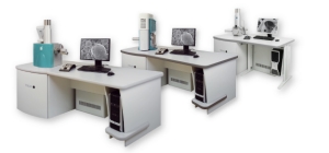
March 8, 2011 – BUSINESS WIRE — TESCAN, scanning electron microscope and focused ion beam workstation maker, delivered a VEGA 3 scanning electron microscope (SEM) to the Massachusetts Institute of Technology (MIT).
The VEGA 3 SEM will support the undergraduate students in the mechanical engineering program, specifically in the Micro and Nano Engineering lab. This course, co-founded by Dr. Sang-Gook Kim encourages creative thinking through hands-on experience via building, observing and manipulating micro and nano scale structures (MEMS, Microfluidics and Nano Materials).
 The VEGA 3 includes high-performance electronics for faster image acquisition (down to 20ns/pixel) and signal processing, an ultra-fast scanning system with compensated static and dynamic image aberrations, an extended range of scanning modes using the original Wide Field Optics, In-Flight Beam Tracing for real-time beam optimization, updated software control with high level of automation, and built-in scripting for user-defined applications. The proprietary Intermediate Lens (IML) works as an "aperture changer." The column design, without any mechanical centering elements, allows fully automated column set-up and alignment. Live stereoscopic imaging, using the advanced 3D Beam Technology, enables 3D viewing and navigation of micro- and nanoscale subjects. Jaroslav Klima, CEO of TESCAN, noted that the SEM will perform easily in the leading-edge research arena with multiple users.
TESCAN is focused on research, development and manufacturing of scientific instruments and laboratory equipment. Learn more at www.tescan.com
Follow Small Times on Twitter.com by clicking www.twitter.com/smalltimes. Or join our Facebook group

