By Debra Vogler, senior technical editor
Aki Fujimura, chairman & CEO of D2S, provides an update of the eBeam Initiative roadmap in a podcast interview held at the SPIE Advanced Lithography Conference (2/27-3/3/11, San Jose, CA). This year, the e-Beam Initiative is looking to obtain design for e-beam (DFEB) mask proof points with various suppliers and by 2012, it expects to have multiple suppliers validate it.
Listen to Fujimura’s interview: Play Now or Download (iPod/iPhone users)
At the eBeam Initiative’s now annual luncheon at SPIE, Tom Faure, senior technical staff member, Photomask Engineering, Systems and Technology Group, Mask House, IBM, reported on the challenges associated with inverse lithography and its impact on shot count for mask writing at 20nm. Fujimura provides a recap of Faure’s points in his interview, and notes how model-based mask data prep (MB-MDP) can address the issues raised. The trade-off between mask cost/mask yield and wafer quality at 20nm is unacceptable, so practical write times for masks and excellent process margins for the wafers are a must, particularly for SoC fabs. Furthermore, double-patterning and restricted design rules are not going to make the increasing shot count go away.
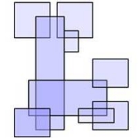
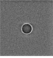
| Overlap shots | Assign dose for each shot | Circle (or any shape) shots |
 |
 |
 |
|
Figure. MB-MDP uses three unique techniques and delivers improved shot count, process window, and built-in MPC. SOURCE: D2S. |
||
|
U.S. Patent 7,579,606; 7,747,997; 7,754,401; 7,759,026; 7,759,027, and other patents pending, D2S, Inc. |
||
Fujimura noted that, because MB-MDP is simulation-based rather than geometry-based (conventional method), it is able to better manage write times. Overlapping shots, assignment of dose for each shot, and any shape shots (character projection), even curvilinear shape shots, are allowed by the technology (see figure).
Among the data Fujimura presented at the luncheon were results obtained from Dai-Nippon Printing Ltd., which showed that for a so-called "impossible mask," the conventional write time of 82hrs could be reduced to 20hrs using MB-MDP.
More from SPIE Advanced Lithography:
- Complementary electron-beam lithography extends optical litho life
- AMAT inspection, Magma yield analysis integration to accelerate litho quals, better chip yields
- SPIE 2011: An ASML review of EUV
- SPIE: A glimpse into Intel’s litho future
- The physics behind Gigaphoton EUV source technology
- Cymer talks EUV source timelines and DUV highlights at SPIE
- EUV, resists, multibeam lithography chat with imec
- SPIE 2011: Where are we now with EUV?
- Carl Zeiss photomask registration correction system, RegC, debuts
- Cymer focus drilling for immersion light sources improves depth of focus by 2x
- Nanometrics launches overlay metrology system, wins order from Asia
- EUV lithography vs EBDW: Interview with Toppan Photomasks at SPIE
- Synopsys lithography verification in Proteus LRC handles EUV, double patterning
- SPIE keynote: Imec installs ASML pre-production EUV scanner NXE:3100
- Brewer Science launches immersion lithography products with OptiStack
Subscribe to Solid State Technology/Advanced Packaging.
Follow Solid State Technology on Twitter.com via editors Pete Singer, twitter.com/PetesTweetsPW and Debra Vogler, twitter.com/dvogler_PV_semi.

