Spincasting-nanoparticles-into-thin-films

March 31, 2011 — Researchers from North Carolina State University have investigated the viability of a technique called spincasting for creating thin films of nanoparticles on an underlying substrate, creating materials with a variety of uses, from optics to electronics.

Spincasting, which utilizes centrifugal force to distribute a liquid onto a solid substrate, already has a variety of uses. For example, it is used in the electronics industry to deposit organic thin films on silicon wafers to create transistors.
Click to Enlarge

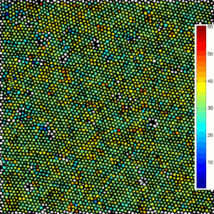
Figure. This is an orientation map of a spin-cast array of FePt nanoparticles. Most nanoparticles are enclosed by a hexagon of six neighboring nanoparticles. Each nanoparticle was color coded according to the angle (in degrees) of the hexagon’s orientation.

For this study, the researchers first dispersed magnetic nanoparticles coated with ligands into a solution. The ligands, small organic molecules that bond directly to metals, facilitate the even distribution of the nanoparticles in the solution and, later, on the substrate itself.

A drop of the solution was then placed on a silicon chip that had been coated with a layer of silicon nitride. The chip was then rotated at high speed, which spread the nanoparticle solution over the surface of the chip. As the solution dried, a thin layer of nanoparticles was left on the surface of the substrate.

Using this technique, the researchers were able to create an ordered layer of nanoparticles on the substrate, over an area covering a few square microns.

Dr. Joe Tracy, an assistant professor of materials science and engineering at NC State and co-author of a paper describing the study, explained that one benefit of spincasting is that it is a relatively quick way to deposit a layer of nanoparticles. "It also has commercial potential as a cost-effective way of creating nanoparticle thin films," Tracy says.

However, the approach still faces several hurdles. Tracy notes that modifications to the technique are needed, so that it can be used to coat a larger surface area with nanoparticles. Additional research is also needed to learn how, or whether, the technique can be modified to achieve a more even distribution of nanoparticles over that surface area.

Analysis of the nanoparticle films created using spincasting led to another development. The researchers adapted analytical tools to evaluate transmission electron microscopy (TEM) images of the films they created. One benefit of using these graphical tools is their ability to identify and highlight defects in the crystalline structure of the layer. "These methods for image analysis allow us to gain a detailed understanding of how the nanoparticle size and shape distributions affect packing into monolayers," Tracy says.

The paper, "Formation and Grain Analysis of Spin Cast Magnetic Nanoparticle Monolayers," was published online March 24 by the journal Langmuir. The paper was co-authored by Tracy; NC State Ph.D. student Aaron Johnston-Peck; and former NC State post-doctoral research associate Dr. Junwei Wang. The research was funded by the National Science Foundation, the U.S. Department of Education, and Protochips, Inc.

Abstract: Ligand-stabilized magnetic nanoparticles (NPs) with diameters of 4-7 nm were spin cast into monolayers on electron-transparent silicon nitride (SiN) substrates. SiN membranes facilitate detailed high-resolution characterization of the spin-cast monolayers by transmission electron microscopy (TEM) and approximate spin casting onto wafers. Suspending the NPs in hexanes and pretreating the substrate with ultraviolet light and ozone (UVO) gives the best results. Computer-aided analysis of the arrays elucidates their grain structures, including identification of the grain boundaries and defects and measurements of the grain orientations and translational correlation lengths. Narrow NP size distributions result in close-packed arrays with minimal defects and large grains containing thousands of NPs. Edge dislocations, interstitials, vacancies, and overlapping NPs were observed. Deviations from close packing occur as the normalized standard deviation of the sample’s size distribution increases above approximately 11%. Polydisperse size distributions and deviations from spherical NP shapes frustrate assembly and prevent ordered packing.
Access: http://pubs.acs.org/doi/abs/10.1021/la200005q

NC State’s Department of Materials Science and Engineering is part of the university’s College of Engineering.

POST A COMMENT

Easily post a comment below using your Linkedin, Twitter, Google or Facebook account. Comments won't automatically be posted to your social media accounts unless you select to share.

Spincasting nanoparticles into thin films

March 31, 2011 — Researchers from North Carolina State University have investigated the viability of a technique called spincasting for creating thin films of nanoparticles on an underlying substrate, creating materials with a variety of uses, from optics to electronics.

Spincasting, which utilizes centrifugal force to distribute a liquid onto a solid substrate, already has a variety of uses. For example, it is used in the electronics industry to deposit organic thin films on silicon wafers to create transistors.

Click to Enlarge

Figure. This is an orientation map of a spin-cast array of FePt nanoparticles. Most nanoparticles are enclosed by a hexagon of six neighboring nanoparticles. Each nanoparticle was color coded according to the angle (in degrees) of the hexagon’s orientation.

For this study, the researchers first dispersed magnetic nanoparticles coated with ligands into a solution. The ligands, small organic molecules that bond directly to metals, facilitate the even distribution of the nanoparticles in the solution and, later, on the substrate itself.

A drop of the solution was then placed on a silicon chip that had been coated with a layer of silicon nitride. The chip was then rotated at high speed, which spread the nanoparticle solution over the surface of the chip. As the solution dried, a thin layer of nanoparticles was left on the surface of the substrate.

Using this technique, the researchers were able to create an ordered layer of nanoparticles on the substrate, over an area covering a few square microns.

Dr. Joe Tracy, an assistant professor of materials science and engineering at NC State and co-author of a paper describing the study, explained that one benefit of spincasting is that it is a relatively quick way to deposit a layer of nanoparticles. "It also has commercial potential as a cost-effective way of creating nanoparticle thin films," Tracy says.

However, the approach still faces several hurdles. Tracy notes that modifications to the technique are needed, so that it can be used to coat a larger surface area with nanoparticles. Additional research is also needed to learn how, or whether, the technique can be modified to achieve a more even distribution of nanoparticles over that surface area.

Analysis of the nanoparticle films created using spincasting led to another development. The researchers adapted analytical tools to evaluate transmission electron microscopy (TEM) images of the films they created. One benefit of using these graphical tools is their ability to identify and highlight defects in the crystalline structure of the layer. "These methods for image analysis allow us to gain a detailed understanding of how the nanoparticle size and shape distributions affect packing into monolayers," Tracy says.

The paper, "Formation and Grain Analysis of Spin Cast Magnetic Nanoparticle Monolayers," was published online March 24 by the journal Langmuir. The paper was co-authored by Tracy; NC State Ph.D. student Aaron Johnston-Peck; and former NC State post-doctoral research associate Dr. Junwei Wang. The research was funded by the National Science Foundation, the U.S. Department of Education, and Protochips, Inc.

Abstract: Ligand-stabilized magnetic nanoparticles (NPs) with diameters of 4-7 nm were spin cast into monolayers on electron-transparent silicon nitride (SiN) substrates. SiN membranes facilitate detailed high-resolution characterization of the spin-cast monolayers by transmission electron microscopy (TEM) and approximate spin casting onto wafers. Suspending the NPs in hexanes and pretreating the substrate with ultraviolet light and ozone (UVO) gives the best results. Computer-aided analysis of the arrays elucidates their grain structures, including identification of the grain boundaries and defects and measurements of the grain orientations and translational correlation lengths. Narrow NP size distributions result in close-packed arrays with minimal defects and large grains containing thousands of NPs. Edge dislocations, interstitials, vacancies, and overlapping NPs were observed. Deviations from close packing occur as the normalized standard deviation of the sample’s size distribution increases above approximately 11%. Polydisperse size distributions and deviations from spherical NP shapes frustrate assembly and prevent ordered packing.
Access: http://pubs.acs.org/doi/abs/10.1021/la200005q

NC State’s Department of Materials Science and Engineering is part of the university’s College of Engineering.

POST A COMMENT

Easily post a comment below using your Linkedin, Twitter, Google or Facebook account. Comments won't automatically be posted to your social media accounts unless you select to share.