By Debra Vogler, senior technical editor
March 21, 2011 — Speaking at the SEMATECH Design for Reliability Workshop: Stress Management for 3D ICs using TSVs (March 17, Santa Clara, CA), Victor Moroz, a scientist at Synopsys, presented results of the company’s collaboration with imec (e.g., Figs. 1-3).
Listen to Moroz’s interview: Download (iPhone/iPod users) or Play Now
In a podcast interview, Moroz explained that there are some strong effects due to stress that cannot be neglected, but taking these effects into account is doable. "Due to the mismatch between copper and silicon, the stress is not that high (100s of megapascals) — it’s lower than what you intentionally put there using stress engineering," he said.
 |
|
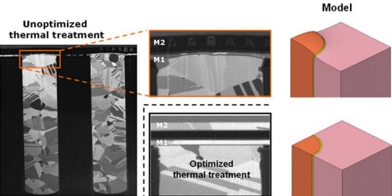
Figure 1. Copper pumping effect: Un-optimized TSV process leads to excessive copper pumping and destroys interconnects around it. Optimized TSV process is demonstrated to not disturb M1 and M2 interconnect layers. SOURCE: Synopsys |
The difference with through silicon vias (TSVs) is that the "stress range is comparable to the size of the TSV." He noted, for example, that if a TSV is 40µm deep, then the stress range is comparable, i.e., tens of microns. "What we found is that for analog transistors, we see a change of up to 5%, and for digital transistors a change by up to 20-30% next to the TSV."
 |
|
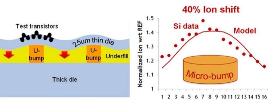
Figure 2. Micro-bump stress effect: The underfill shrinks considerably and pulls the thin die along in between the rigid copper micro-bumps. The thin die warps around the micro-bumps and strains the transistors. Test NFETs on top of the micro-bump exhibit 40% higher current compared to the reference NFETs that are far from micro-bumps. SOURCE: Synopsys |
He added that the stress effect decays very slowly for analog transistors; the keep out zone can be tens of microns. For digital transistors, however, the effect is stronger, but it acts over a shorter range. Still, Moroz noted that these effects are not showstoppers.
 |
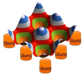
| Figure 3. Calculated warping of the thin die (vertical scale exaggerated). Thin die goes up above the Cu micro-bumps, forming hills there, with valleys and saddles in between the micro-bumps. The Si-calibrated model can be used to account for TSV and micro-bump stress effects and design reliable 3D ICs. SOURCE: Synopsys |
Subscribe to Solid State Technology/Advanced Packaging.
Follow Advanced Packaging on Twitter.com by clicking www.twitter.com/advpackaging. Or join our Facebook group<

