April 1, 2011 — Scientists at the National Institute of Standards and Technology (NIST) have developed a way to measure the wear and degradation of the microscopic probes used to study nanoscale structures in situ and as it’s happening. Their technique can speed up and improve the accuracy of the most precise and delicate nanoscale measurements done with atomic force microscopy (AFM).
 |
|
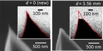
Image. As an atomic force microscope’s tip degrades, the change in tip size and shape affects its resonant frequency. That can be used to accurately measure, in real time, the change in the tip’s shape. Credit: Jason Killgore, NIST |
Today, most researchers stop the measurement to "take a picture" of the tip with an electron microscope, a time-consuming method prone to inaccuracies.
NIST materials engineer Jason Killgore has developed a method for measuring in real time the extent to which AFM tips wear down. Killgore measures the resonant frequency of the AFM sensor tip, a natural vibration rate like that of a tuning fork, while the instrument is in use. Because changes to the size and shape of the tip affect its resonant frequency, he is able to measure the size of the AFM’s tip in increments of a tenth of a nanometer, essentially atomic scale resolution. The technique, called contact resonance force microscopy, is described in a paper recently published in the journal Small. (J. P. Killgore, R. H. Geiss and D. C. Hurley. Continuous measurement of AFM tip wear by contact resonance force microscopy. Small. Published March 15, 2011.)
Knowing how fast and to what extent the tip is being worn away during the measurement has been the challenge for researchers and manufacturers trying to create images of the surfaces of nanomaterials and nanostructures. Taking a photo is impossible at such small scales, so researchers use atomic force microscopes to measure peaks and valleys as it’s dragged back and forth across a surface. These devices are used extensively in nanoscale imaging to measure the contours of nanostructures, but the AFM tips are so small that they tend to wear down as they traverse the surface being measured.
Thousands of AFMs are in use at universities, manufacturing plants and research and development facilities around the world. Improving their ability to measure and image nanosized devices will improve the quality and effectiveness of those devices. Another benefit is that developing new measurement tips — and studying the properties of new materials used in those tips — will be much easier and faster, given the immediate feedback about wear rates.
The National Institute of Standards and Technology (NIST) is an agency of the U.S. Commerce Department.
Follow Small Times on Twitter.com by clicking www.twitter.com/smalltimes. Or join our Facebook group

