T. Onishi, managing director, Grand Joint Tech, Ltd. and E.J. Vardaman, president, TechSearch International, Inc.
April 21, 2011 — While lovely pale pink blossoms slowly floated down from ancient cherry trees in Nara, Japan, almost 300 leaders in the modern world of electronics packaging met to discuss the latest technology developments in semiconductor packaging and interconnect at the International Conference on Electronics Packaging (ICEP) held in Nara, Japan, April 13-15.
ICEP featured keynotes from:
- Dr. Claudius Feger of IBM’s Thomas J. Watson Research Center on "Opportunities in the Brazilian Microelectronics Market,"
- Dr. John Lau of the Electronics & Optoelectronics Labs (EOL) at the Industrial Technology Research Institute (ITRI),
- Dr. Taejoo Hwang of Samsung Electronics on "3D Package for Mobile Application,"
- Professor Kazuaki Yazawa of the Baskin School of Engineering at the University of California Santa Cruz, and
- Jan Vardaman, TechSearch International, Inc. on "Advanced Packaging the New Decade."
Low-k dielectrics
Packaging and assembly of low-k and ultra low-k (ULK) wafers was an important topic of discussion. Several presentations, including one from ASE, discussed methods to minimize the potential for extreme low-k (ELK) delamination in flip chip packages. The work focused on the ratio of the polyimide opening over UBM size, the use of a thick RDL as a stress buffer, a thick substrate core, and a thin die to minimize the ELK delamination potential. A paper from IBM focused on the mechanical integrity of ultra fine pitch wire bond on ELK devices. Thickness of SiO2/FTEOS layer and via density in the ELK layer were determined to be key factors in establishing good wire bond integrity.
Copper pillar
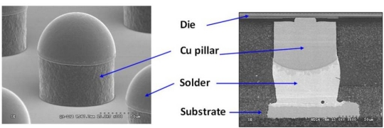
The tremendous interest in copper pillar (also called Cu pillar and copper post) was evident at ICEP with a standing-room-only crowd listening to ASE’s presentation on its plans for Cu pillar in FC-CSPs. Figure 1 shows the structure.
 |
| Figure 1. ASE copper pillar structure. |
ASE presented reliability data from test on a 5 × 5mm 65nm-technology die with 150µm bump pitch packaged in a 10 × 10mm package. ASE reported that it passed 3,000 hours of high temperature storage test at 150°C and 3,000 hours of thermal cycling test at -55 to +125°C. Results were also reported for a 40nm-technology 10 × 10mm die with 162µm bump pitch packaged in a 31 × 31mm form factor. The part passed 2,500 hours of -55 to +125°C thermal cycling test.
Wafer-level packaging (WLP)
Wafer level packaging remains a hot topic, with Hynix presenting its WLP developments for high-speed memory and ASE’s presentation on its fan-out packaging (FOWLP) for multi die.
 |
| Figure 2. ASE FOWLP. |
Figure 2 shows a fan-out package from ASE.
3D IC
3D packaging presentations were sprinkled throughout the conference. Many discussions in sessions and around the conference site focused on 3D TSV technology developments. A new test method to determine thin silicon die strength was presented by researchers from Chang Gung University in Taiwan. Researchers at ITRI presented their developments of wafer-level underfill bonding process for 3D chip stacking.
Too many package choices
With so many packaging choices, it has become difficult to select the appropriate package for the application. A presentation from IBM Japan proposed a methodology for packaging selection for mobile products. Choices included wire bond and flip chip chip scale packages (CSPs), quad flat pack no leads (QFNs), and WLPs (both conventional and fan-out).
Reliability matters
Reliability for all types of packages was discussed by many companies including Powertech Technology, Inc., Toshiba, NAMICs, Sanyu Rec, and Sony.
E.J. Vardaman is president and founder of TechSearch International, Inc. a company involved in analyzing technology and market trends in semiconductor packaging, materials and assembly since 1987. Learn more at www.techsearchinc.com
Subscribe to Solid State Technology/Advanced Packaging.
Follow Advanced Packaging on Twitter.com by clicking www.twitter.com/advpackaging. Or join our Facebook group

