By Debra Vogler, senior technical editor
April 14, 2011 — Shyng-Tsong Chen, lead integrator for back-end integration at IBM (Albany Nanotechnology Center), will be presenting "64nm pitch Cu dual-damascene interconnects using pitch-split double-exposure patterning scheme" at the IITC 2011 Conference (coming up in May 9-12, Dresden, Germany). This technology will be needed for back end of line (BEOL) interconnects beyond 22nm devices.
In this podcast interview (Listen: Download or Play Now ) Chen gives an in-depth summary of the work and discusses its extendibility to 56nm-pitch interconnects.
 |
|
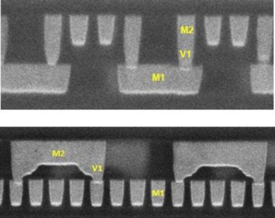
Figure. Via chain SEM cross-section along M1 line direction (upper) and along M2 line direction (lower). |
The research was motivated by enabling sub-80nm-pitch patterning. The group used a self-aligned via (SAV) lithography/reactive ion etch (RIE) scheme to create vias confined by line trenches. According to the paper, an undercut-free post-RIE trench profile enabled good metal fill. The figure shows post-chemical-mechanical planarization (CMP) cross-section scanning electron microscopy (SEM) images along the M1 line and M2 line directions. As noted in the paper, the upper image shows that the V1 via size is defined by the M2 line above as a result of the SAV process. The lower image shows the V1 via tapered along the M2 line direction.
Also see our IITC preview interview about chip/package stress detection work at Stanford University.
Subscribe to Solid State Technology/Advanced Packaging.
Follow Solid State Technology on Twitter.com via editors Pete Singer, twitter.com/PetesTweetsPW and Debra Vogler, twitter.com/dvogler_PV_semi.

