April 12, 2011 — Sonoscan, Inc., acoustic micro imaging systems maker, has demonstrated the single-scan imaging of a sample at 50 different depths, or gates. The technique, called PolyGate, yields 50 images that show internal features at each depth of the package.
In conventional imaging, much wider gates are used to confine imaging to a single depth of interest such as the die face or leadframe depth. The ability to set multiple gates that are imaged simultaneously during a single scan gives the system user the ability to see internal features at each gate, and to see how features, including defects, change from one gate to the next.
 |
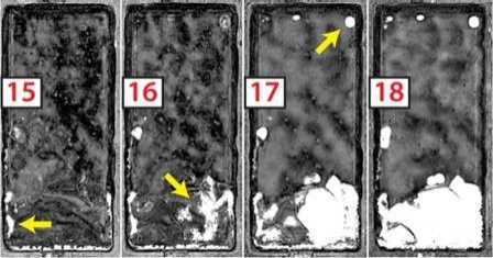
Shown in the image are gates 15 through 18 (out of 50) imaging downward from the top surface of a ceramic chip capacitor that is 3.18mm thick. Each gate is about 60µm thick. PolyGate can set up to 200 gates, and Sonoscan has demonstrated 5µm gates in some materials.
Bright white regions in the acoustic image are defects. Small edge delaminations exist at Gate 15, but at Gate 16 a larger defective area appears in the lower right. In Gate 17 this area blossoms into a large delamination or void, and small voids appear at the top. The abruptness with which the large feature appears in Gates 17 and 18 suggests that the feature is very flat.
Sonoscan Inc. develops and manufactures acoustic microscopes and sophisticated acoustic micro imaging systems, widely used for nondestructive analysis of defects in industrial products and semiconductor devices. Sonoscan can be contacted at www.sonoscan.com.
Subscribe to Solid State Technology/Advanced Packaging.
Follow Advanced Packaging on Twitter.com by clicking www.twitter.com/advpackaging. Or join our Facebook group

