by James Montgomery, news editor
May 17, 2011 – Bob Krakauer, CFO of GlobalFoundries, offered a strategic overview for investing in semiconductor manufacturing, in his presentation at this week’s ConFab gathering in Las Vegas (Monday 5/16).
World GDP growth is really two trendlines, with emerging economies (Asia, Latin America, Eastern Europe) pulling up the overall average. And in the semiconductor industry, the foundry sector is outpacing overall growth (though 2010 was a close exception for fabless sales).
Products are shifting to emphasize mobility and connectivity, as multifunctional devices proliferate packed with capabilities for communication, computing, entertainment (including video), and navigation. Embedded and motion processing are key functions.
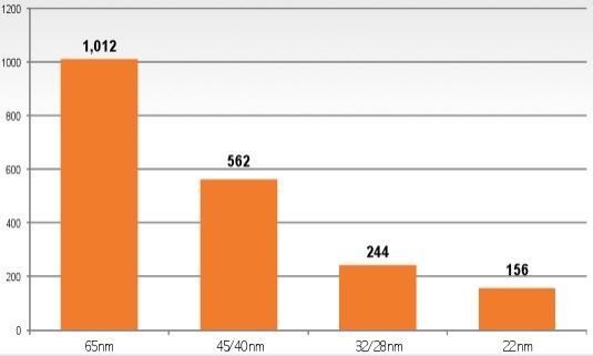
Specifically to the manufacturing side, Krakauer tracked the increasingly packed-in advancements from 4Xnm to 3Xnm (immersion, low-k, strained Si, HKMG) to 2Xnm (source-mask optimization, maybe EUV?) to 16nm/14nm (nonplanar structures and 3D integration). All of these are creating an "explosion" of innovations in materials, lithography, and architectures — and that translates directly to rising costs. Design costs have surged around ~50% per node since the 65nm node, and now amount to $140M design cost for 22nm. Not surprisingly, there are connections to R&D spending (rising fast since 2008) as well as design starts, which have declined 35%-50%+ per node during the same timeframe.
 |
 |
 |
| (top) Design cost in $M. (mid) R&D as a percentage of revenue. (btm) Design starts (first five years). |
Nevertheless, demand for capacity continues to grow. Low-power 28nm HKMG technology will enable continued expansion, Krakauer noted. He showed it as an interrelated cycle of "endpoint" devices/people, content/services, and traffic/bandwidth; three billion 3G subscribers projected in 2014, mobile traffic doubling every year (39× growth from 2009-2014), with Internet video dominating IP traffic (48% CAGR.)
The industry landscape is being redefined, Krakauer noted, as the fab-lite/fabless movement rolls on. OEMs, key foundry customers, are driving systems-based offerings, and recent M&A activity (Qualcomm/Atheros, TI/National) is pushing segment/customer consolidation. Consolidation also is arriving on the manufacturing end, as rising capital intensity and sub-28nm technology trends require greater supply chain-wide collaboration, from early-stage research through design and manufacturing, involving customers, partners, academia, and even competitors.
The foundry of the future, Krakauer noted, will be: customer- and product-centric, provide technology and cost leadership, build on a collaborative model (across all supply-chain segments), with capability and vision to invest and build through industry cycles, and with a global footprint to minimize risk and "maximize customer value."
As for GlobalFoundries’ long-term investments, Krakauer pointed to the firm’s current market share (~13%, No.3), plans for doubling capex in 2011 to $5.4B (about 120% of revenue), and several investment focuses: 200mm capability/capacity, expansion at Fab 1 in Dresden, and ongoing construction/tooling forthcoming 300mm Fab 8 in upstate New York. (Quick facts about Fab 8: It’s a $4.6B 300mm fab designed for up to 3 modules, with six football fields of cleanroom space [bigger than the Chrysler Building], expected to come online in late 2012, ultimately with 60,000 WSPM. The local Times-Union has a photo tour here.)
Krakauer also detailed plans to develop a technology cluster near the Abu Dhabi airport, where GlobalFoundries will "play key near-term and long-term roles" from sharing best practices to establishing a technology and manufacturing presence.

