Meredith Courtemanche, digital media editor
May 16, 2011 — Today at The ConFab, John Chen (Nvidia), Jeong-ki Min (Samsung Electronics), and Abraham Yee (Nvidia) gathered foundry, OSAT, and chip maker leaders to discuss what happens beyond Moore’s Law. The following are key points from "Collaboration to Strengthen the IC Supply Chain."
John Waite, VP, packaging development and central engineering at GLOBALFOUNDRIES, presented "Supply Chain Reaction: A Collaborative Approach to Packaging Innovation." Since packaging costs are the dominant contributor to the value chain, designers need to select the right combination of silicon and packaging technologies to achieve performance and cost goals.
What enables success in the More Moore realm? Waite lists diverse options for wafer bumping (lead-free, copper pillar, lead and high-lead solders used in bond on pad, repassivation or redistribution [RDL] designs) and package form factor (QFP/QFN, BGA and flip chip, wafer-level chipscale packages [WLCSP]), as well as vertical options that take advantage of Z space (stacked chips, system in package [SiP]). These each have tradeoffs of cost, time, and density/performance, and customers must make packaging choices with these goals in mind.
 |
| Packaging influences the front end. SOURCE: John Waite, GLOBALFOUNDRIES. |
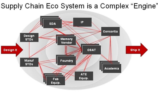
Packaging increasingly requires attention on the frontend because of the packaging demand on the wafer. The frontend, backend, and system suppliers must collaborate in chip development. Early engagement, EDA tool flow optimization, turnkey wafer-to-package assembly, and other risk reduction strategies take a design from R&D into high-volume manufacturing.
Nick Yu, VP of technology development, Qualcomm, brought a fabless perspective to the session. In "3D Through Si Stacking Technology — a Qualcomm Perspective," Yu reminds us that 3D packaging creates thin, small, exciting products with long battery life. All 3D packages create better form factors on the board, increased performance for the device, and higher modularity in the design. The options to create a 3D package, however, as Waite also noted, are myriad: wire bonded chip stacks, flipped stacked chips, bumped/bonded chip stacks, through silicon vias (TSV) implemented as interposers, via first, or mid-process. Yu assesses these 3D technologies on the commercialization roadmap. Leading-edge technologies, like wide I/O memory on logic, are moving from lab to fab for the best of all worlds.
 |
| Supply chain needs a 3D ecosystem, as 3D is disruptive to how we do things today. SOURCE: Nick Yu, Qualcomm. |
While integrated fabless companies are ramping up leading-edge 3D IC designs, the lack of standards is holding back the 3D ecosystem. Traditional business models also don’t support the boundary-breaking 3D design and process steps. Yu supports integration via standards bodies and research consortia to bring design and manufacturing standards to the 3D arena. Consider Yu’s questions: Who owns the die? Who holds the inventory? How are pass-through costs funded? Who owns the integration process? Who owns the yield? Is the additional risk of TSV worth the benefits over wire-bonded stacks? Is a fabless design company or an IDM the way to go? The key question here is who acts as the "3D aggregator"? Foundry, memory company, OEM, fabless, OSAT?
Raj Pendse, VP of product and technology marketing at STATS ChipPAC and Robert Darveaux, CTO of Amkor, covered this supply chain integration from the dedicated packaging house perspective. Pendse presented "3D Packaging Evolution from an OSAT Perspective." Darveaux spoke on "Supply Chain Challenges for 3D Integration of Memory and Logic Devices using TSVs."
 |
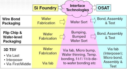
| Material flow and infrastructure evolution. SOURCE: Dr. Raj Pendse, STATSChipPAC Inc. |
Pendse sees synergies and intersections among parallel developments in the three areas of packaging technology (i.e. traditional die and package stacking on substrates, fan-in and fan-out wafer level packaging and 3D Si integration). With these new process technologies, the OSAT industry’s role is transformed. Pendse channels wafer bumping, thinning, and other tasks into an in-between space for the Si foundry and OSAT to determine logical hand off points. Many of these processes can be done in both — the question to ask is who can do it better in each scenario? Is TSV fabrication best handled in the fab, with the OSAT taking over via fill and silicon interconnect? Pendse also spoke on "bridge" technologies — interposers, super-thin package-on-package, TSV hybridized with fan-out wafer-level packages (FOWLP) — that play an interim role in the commercialization of 3D. Pendse shared a typical OSAT TSV roadmap through 2013 with the attendees.
Darveaux compared the relative ease of sourcing, assembly, and test of package-on-package (POP) with the challenges of TSV: difficult to test high-density area array contact pads or bumps; bare or partially assembled memory and logic die that are difficult to burn in adequately; a newer joining technology not widely available to OEMs and contract assemblers; a poorly characterized joining process yield; and, due to the immaturity of the test, burn-in, and assembly; unclear ownership of defect liability. This applies to the "2.5D" interposer strategy as well as pure 3D TSV stacks. Interconnect processes are too new and done in too small sample sizes to lead to industry agreement on the right method: die-to-die first or die-to-laminate first? Interposer in singulated format or wafer format?
 |
 |
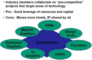
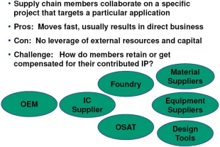
| Consortium collaboration model. | Supply chain collaboration model. SOURCE: Robert Darveaux, Amkor Technology. |
These problems can not be resolved by technologies or business models alone. TSV processes can be standardized and characterized, with the resource-sharing model of consortia or the faster but potentially messy supply chain collaboration on specific projects. Both offer pros and cons, and fit different needs of the industry.
More from The ConFab:

