Radovan Faltus, AVX spol.s.r.o.
May 1, 2011 — With proper design, a solid state drive (SSD) is able to provide high data transfer rates, low access time, improved tolerance to shock and vibration, and reduced power consumption. For some applications, the improved performance and durability outweigh the higher cost of an SSD relative to a hard disk drive (HDD). However, flash memory can wear out. Fortunately, the wear-out physics are well understood and data management strategies are used to compensate for the limited lifetime of flash memory. Key to SSD performance is the SSD controller, which controls how read and write operations are performed to maximize data transfer speed and disk life.
Floating gate flash memory
A floating gate memory cell, the basic unit of flash memories, is a type of metal-oxide-semiconductor field-effect transistor (MOSFET). MOS transistors work by forming an electrically conductive channel between the source and drain terminals. When a voltage is applied to the control gate, an electric field causes a thin, negatively charged channel to form at the boundary of the SiO2 and between the source and drain regions. When the N-channel is present, electricity is easily conducted from the source to the drain terminals. When the control voltage is removed, the N-channel disappears and no conduction takes place. The MOSFET operates like a switch, either in an "on" or "off" state.
Erasing the contents of a memory cell is performed by placing a high voltage on the silicon substrate while holding the control gate at zero. The electrons stored in the floating gate tunnel through the oxide barrier into the positive substrate. Thousands of memory cells are etched onto a common section of the substrate, forming a single block of memory. All of the memory cells in the block are simultaneously erased when the substrate is ‘flashed’ to a positive voltage. An erased memory cell will allow N-channel formation at a low control gate voltage because all of the charge in the floating gate has been removed. This is referred to as logic level 1 in a single-level cell (SLC) flash memory cell.
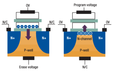 |
| Figure 1. Erasing and programming the contents of a MOSFET memory cell. |
The cell is programmed by placing a high voltage on the control gate while holding the source and drain regions at zero. The high electric field causes the N-channel to form and allows electrons to tunnel through the oxide barrier into the floating gate. Programming the memory cells is performed one word at a time (i.e., cell by cell) and usually an entire page (e.g., 2048 bytes) is programmed in a single operation. A programmed memory cell inhibits the control gate from forming an N-channel at normal voltages because of the negative charge stored on the floating gate. To form the N-channel in the substrate, the control gate voltage must be raised to a higher level; this is referred to as logic level 0 in an SLC flash memory cell.
NAND flash block architecture
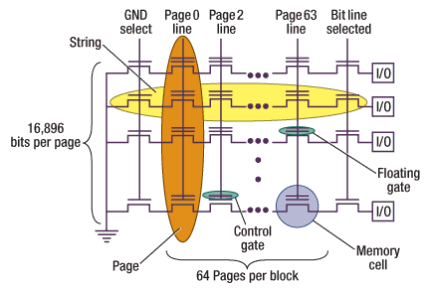
Flash memory cells are organized into a hierarchy of bytes, pages, blocks and planes. The organization of one type of 4 Gigabit (Gb) SLC NAND flash memory chip is shown in Figure 2.
 |
|
Figure 2. NAND flash block architecture example. |
NAND flash memory chips arrange the memory cells in a logical ‘not-and’ (NAND) configuration. This arrangement strings together all of the cells for a common input/output (I/O) bit across all memory pages. Because of this arrangement, it is not possible to directly access individual data bytes within a memory page. The flash memory controller must read an entire page of memory from the device. Also, an entire page must usually be programmed at once, although some devices permit partial page programming. That makes NAND flash unsuitable for most random byte-access memory applications.
NOR flash memory is less densely packed on the silicon due to the space required for all of the I/O bit lines and ground connections. NOR flash memory has a corresponding higher cost per bit than NAND flash memory. Because NOR flash memory allows random byte access, it can be used as program storage for microcontrollers.
Endurance
HDDs have no effective limit on the number of writes that can be performed. NAND flash, on the other hand, can only be written to a finite number of times. This is known as endurance.
Looking at the two categories of NAND flash:
- Single level cells, (SLC) where each cell has one of 2 states representing 1 bit, has a typical endurance of 100,000 writes.
- Multi-level cells, (MLC), where each cell has one of 4 voltage levels representing 2 bits/cell. The penalty for this greater density is a lower endurance, typically 10,000 writes.
The endurance limit means that the SSD controller must spread write operations evenly throughout the NAND flash blocks (wear leveling), to prevent parts of the memory failing prematurely. Wear leveling means that files are not written in sequential blocks, adding complexity to the file allocation table (FAT) and SSD management system, which must, as a consequence, keep track of which physical blocks a file has been written to and which blocks to use next.
Speed
Conventional HDDs are limited in their input/output (I/O) performance by the need to move the read/write heads.
SSDs, on the other hand, have NAND flash limitations:
- A location must be erased before it is written to;
- Erase operations are performed on entire blocks; and
- Read and Write operations are by page.
SSDs are not limited to individual NAND flash IC performance. Figure 3 shows a block diagram of a typical SSD. The NAND flash ICs are partitioned in several banks and the controller can interleave operations between banks. For example, one group can be read while another is being erased, or multiple blocks can be erased simultaneously. This greatly increases throughput.
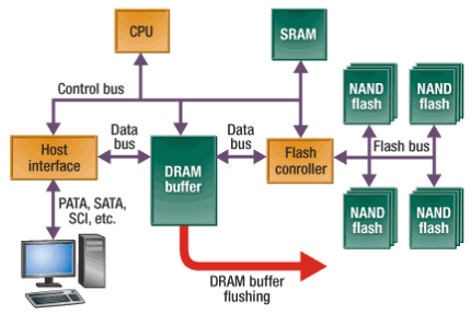 |
| Figure 3. Typical SSD block diagram. |
On the data bus, data received is transferred from the host interface into a synchronous dynamic random access memory (DRAM) buffer. From there, data is flushed and routed to the flash controller, which writes the data into flash memory. Similarly, a read command along with the logical address is sent to the CPU via the host interface chip. The CPU determines the physical address of memory from the mapping table and sends the information to the flash controller chip so that the data can be accessed and sent to the host interface. From there, the data is sent to the host.
A DRAM buffer improves read/write speed of SSDs
In the enterprise market, data integrity is paramount and high data transfer rates are extremely important. To ensure maximum data transfer speed while ensuring no data loss in the event of a power failure, use a powerful SSD controller with DRAM buffer and power supply backup. In this way the maximum data speeds for the latest NAND SLC flash memory products increases from 166MB/s to around 260MB/s.
SSD power supply backup options
Several options for power backup source device are available:
- Secondary battery: Simple solution, but the limitation is a relatively short lifetime — about 500 cycles — and high price, especially when integrated into the IC package.
- Supercapacitor: Although these devices can offer a high capacitance and store enough energy for DRAM buffer flushing into the flash memory, they have a relatively high ESR, which effectively limits energy flow. Another consideration with most supercapacitor technologies is their narrow working temperature range — usually up to 70°C only — which eliminates the possibility of standard automated linear reflow soldering. Therefore, most supercapacitors must be hand soldered, increasing assembly time and costs.
- Tantalum capacitor: When stacked in parallel, these simple parts exhibit enough capacitance to deliver the energy needed for data flushing. Tantalum capacitors offers a wide operating temperature range (up to 125°C) and are compatible with standard, automated lead-free reflow soldering processes. They are also very reliable.
Designing a power supply for an SSD
The backup supply for an SSD must provide sufficient power to transfer essential data from the fast DRAM buffer memory into non-volatile flash memory should the power fail. For effective SSD power backup design the correct selection of input DC/DC controller is important.
When a capacitor is being used as an energy reservoir, its voltage drops as its energy drains. Therefore, the first step DC/DC converter in an SSD power system should be a Buck-Boost type, which is able to step up the voltage at the end of capacitor discharge period (Figure 4).
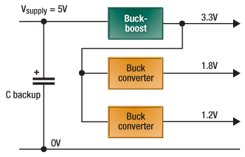 |
| Figure 4. Typical SSD power supply section block diagram. |
Capacitor parameters used in backup applications
The following paragraphs analyze the impact of backup capacitor parameters on backup performance, measured by backup time, tb, the time taken for the capacitor to completely discharge from full charge state.
Considering the example of a modern SSD with 5V supply voltage and reduced power consumption, P, (in data write mode) of 0.22W. DRAM buffer memory size is typically 64MB. If the speed of data write into flash memory is 140MB/s, the minimum time for full buffer flushing from DRAM to flash, tf, is given by:
tf = memory size/write speed = 457ms.
Obviously, the backup time that must be provided by the reservoir capacitor to enable full buffer flushing into the flash memories of the SSD needs to be bigger than the flash time.
tb > tf
It is useful to simulate the capacitor discharging process based on constant power consumption and energy flowing to the input of the Buck-Boost converter. Such a simulation can use mathematical or equivalent circuit models. The input conditions are: fully charged capacitor with Uci = 5V, power consumption Pc and disconnection from external power supply in time
t = 0s
The end of useful backup function will differ depending on used DC/DC. For simplification we consider capacitor discharge to Uc = 0V (ideal converter or energy harvester).
The basic capacitor formula for current is:
I = C*dU/dt
where current I is given by the constant current consumption, I = P/U, which will naturally grow as the voltage of the capacitor drops.
The effective series resistance (ESR) of the capacitor may affect backup time, tb, due to thermal energy loss. The current draining from capacitor causes an additional voltage drop, therefore, the input DC/DC converter increases the actual value of the current to cover full power demand.
Ucext = Ucint – ESR*I.
In this example, the value of backup capacitor capacitance, C, has been estimated as 9mF. In order to save PCB space, new high capacitance/low profile PulseCap capacitors from AVX were selected for this application. The capacitor stack behaviour has been simulated and compared with other possible capacitor technologies.
Possible solution for temperatures to 85°C
To achieve the required 5V operating voltage (up to 85°C operating temperature) and requested capacitance of 9mF, a stack of nine TLN4108M010R0100 1mF PulseCap capacitors can be connected in parallel. These devices have an ESRmax of 100mOhm at 100 kHz and a DCLmax of 100µA at 25°C. Individual capacitors have a footprint of just 7.3 x 6.1mm and 2mm height. They use an undertab construction with solder pads on the under side only.
The required ‘block’ of nine devices measures 21.9 x 18.3 x 2mm.
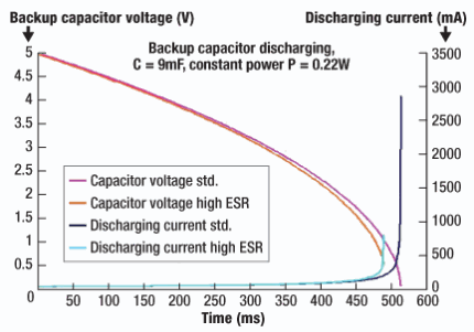 |
| Figure 5. Backup capacitor discharging with ESR impact. |
A first simulation of the discharging energy reservoir with C = 9mF, as specified above and loaded by a constant power, P, of 0.22W shows discharging time = backup time, tb1, = 514ms. (Fig. 5)
The maximum ESR of the stack of capacitors is given by ESRmax @ 100 kHz multiplied by 4.5 (a factor for DC ESR) and divided by 9 for parallel combination.
ESRsmax = 100*4.5/9 = 50mOhm
This is a relatively low figure, so thermal energy losses are negligible, giving a change of backup time to tb2 = 506ms, when the effects of ESR are included.
By contrast, supercapacitors exhibit higher ESR than solid tantalum capacitors, when comparing similar nominal capacitance parts. For example, a BZ05 supercapacitor has an ESRmax of 600mOhm at 1kHz, which is nearly the same for DC conditions. The yellow curve labeled ‘Capacitor voltage high ESR’ in Fig. 6 shows the discharging of such capacitor. The main impact on ESR power loss is experienced during the last phase of discharge when the discharge current is elevated. Simulation shows that the available backup time for supercapacitors, tb3, must be shortened due to the effects of ESR to 490ms.
The leakage current, DCL, of reservoir capacitors causes self-discharging and behaves as an additional load which must be considered on top of energy consumption. The leakage current of the selected TLN4108M010 capacitor stated in the datasheet, DCLmax25, is 100µA (at 25°C, rated voltage, steady state [after 5 minutes]). The worst case (highest) value of DCL in this case is at the highest operating temperature (85°C). A factor of 7.75 can be used for recalculating DCL for 85°C, according to:
DCLmax85 = 7.75*DCLmax25
and factor 9 for parallel combination of 9 capacitors, according to:
DCLmax85s = 9*DCLmax85
The application voltage in this backup application is 50% of rated value or lower, depending on the phase of discharge. Hence the leakage current is reduced with respect to the actual derating factor. (Leakage current estimation is discussed in "Low Leakage Current Aspect of Designing with Tantalum and NbO Capacitors," available at http://www.avx.com.)
The top DCL value for the stack of TLN4108M010 calculated as above is DCL85s1 = 6975µA.
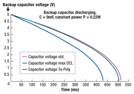 |
| Figure 6. Backup capacitor discharging with DCL impact. |
When the maximum DCL for worst-case operating conditions is considered, the backup time for the TLN4 SMD tantalum capacitors must be reduced from 514ms (tb1) to 504ms (Fig. 6), tb4 — quite a minor difference and likely to be even smaller if we accept that the real leakage currents are typically far below their maximum datasheet limits.
However, if we consider using tantalum polymer capacitors rather than PulseCap TLN4 tantalums, there is a considerable change. Ta-Poly technology capacitors have a much high leakage current (10x DCL) than pure tantalum devices, so DCL85s2 is 69750µA. Such high DCL level significantly affects backup time, shortening tb5 to 430ms.
Results summary
Parameters of the SSD used:
Supply voltage, Vs: 5V
Data write mode power consumption, P: 0.22W
DRAM buffer size: 64MB
NAND Flash data write speed: 140MB/s
Buffer flushing time, tf: 457ms
Proposed backup solution. Stack of 9 parallel TLN4108M010R0100 PulseCap tantalum capacitors (C = 9mF), (capacitance production tolerance not considered).
| Capacitor technology | Effect | Backup time | Condition tb > tf |
| Tantalum Pulsecap | None (ideal capacitor) | tb1 = 514ms | OK |
| Tantalum Pulsecap | ESR (limit conditions) | tb2 = 506ms | OK |
| Supercapacitor | ESR (limit conditions) | tb3 = 490ms | OK |
| Tantalum Pulsecap | DCL (worst conditions) | tb4 = 504ms | OK |
| Tantalum Polymer | DCL (worst conditions) | tb5 = 430ms | Fail |
| Table. Simulation results. | |||
Conclusion
High-speed cache memory greatly improves SSD performance. Providing a power backup for DRAM buffer memory assures no data loss on power off or power failure, and also improves speed and reaction time after power on. Tantalum SMD chip capacitors for this application offer several advantages: high reliability and wide operating temperature range; standard leadfree reflow soldering compatibility; and very low profile when undertab construction is chosen. Using TLN4 capacitors in parallel combination provides a capacitance sufficiently high enough to flush data from the DRAM buffer for low power consumption SSDs if the power fails.. However, tantalum polymer capacitors are not suitable for this reservoir function because of their relatively-high self-discharging. Supercapacitors are limited by a narrower operating temperature range which means they must be hand-soldered; additionally, they are not so effective due to higher ESR, but they can backup well with higher available nominal capacitances.
Radovan Faltus works in the Technical Marketing department at AVX spol s.r.o., Czech Republic.
Also read: Intel throws hat into SSD vs HDD debate
Subscribe to Solid State Technology/Advanced Packaging.
Follow Solid State Technology on Twitter.com via editors Pete Singer, twitter.com/PetesTweetsPW and Debra Vogler, twitter.com/dvogler_PV_semi.

