by Debra Vogler, senior technical editor
May 18, 2011 – Raj Jammy, VP of materials and emerging technologies at SEMATECH, covered a broad swath of CMOS scaling drivers, system and device trends, and infrastructure requirements during session #3 at the ConFab (May 15-18 in Las Vegas). System-level trends, such as smart phones, mobile computing (e.g., iPads), and cloud computing are driving requirements for low- and ultralow-power logic with multi-core/multi-modules, dense 3D nonvolatile memory RAM for SSDs, and dense DRAMs. There is also a move to SoCs, along with high levels of functional integration and faster data transfer between modules and chips.
At the system level, the implications for devices include an even greater need for leakage reduction, and wide-band intra-chip and inter-chip interconnects. At the device level, architectural transitions to 3D FinFETs, III-V FETs, 3D flash memories, RRAM, STTRAM, SoCs, and 3D TSVs, and even photonic interconnects are being evaluated. Each of these alternatives poses specific challenges — but common to all are strong infrastructural needs to be successful. Among the transitions’ challenges will be new materials and/or using non-silicon materials, new models/test methods/designs, integration challenges, as well as processes, materials, tools, and packaging.
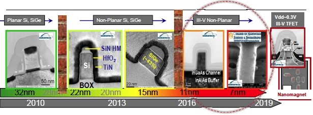
Jammy sees CMOS transitions unfolding between 2012 and 2017 (Figure 1) — starting with planar Si, SiGe (2010), moving to non-planar Si, SiGe in 2013, and on to III-V non-planar in 2016 and Vdd-0.3V III-V TFETs by 2019. Robust process technologies and tools such as selective ALD that are low damage will play a major role in making the transitions happen. Materials interactions and devising suitable test structures, methods and reliability will also be needed.
 |
| Figure 1: Roadmap CMOS transitions, 2012-2017. |
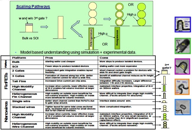
With respect to non-planar device scaling, the pros and cons among the key technologies (i.e., wafer, FinFETs, and nanowires) will have to be weighed. For example, the starting cost for bulk wafers are lower than for SOI wafers, but they require more process steps to produce isolated devices. And the use of FinFETs poses many possibilities: two or three gates, tall fins, a high-mobility channel, or a heterogeneous fin channel. Even nanowires have many pathways from which to choose: single wire, stacked wires, high-mobility channel, or a heterogeneous wire channel — with progressively more difficult integration going from one to the other (Figure 2).
 |
| Figure 2: Non-planar device scaling: trade-offs are key. |
At The ConFab 2011, Jammy spoke with senior technical editor Debra Vogler about TSVs, SoCs, SiPs, logic, and memory:

