FEI plasma FIB tool targets packaging apps

By Debra Vogler, senior technical editor

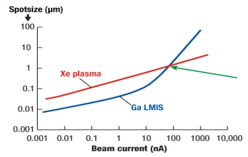
June 13, 2011 — FEI launched its Vion plasma focused ion beam (PFIB) system based on inductively-coupled plasma (ICP) source technology using a xenon ion beam. The system generates more than a micro-amp of beam current and can remove material faster (>20× improvements in speed, Fig. 1) than liquid metal ion sources that typically max out at a few tens of nano-amps, according to the company. Because of its speed, FEI will target new technologies, such as 3D packaging and 3D transistor design technologies, where PFIB analysis is more practical.
Click to Enlarge
  • High-volume milling/high beam current
  • Ga-FIB loses size advantage to plasma source as beam current goes above 50-60 nA
  • Xe has high sputter yield, high brightness, and low energy spread
  • No Ga contamination

Figure 1. Plasma FIB is 20× faster than current FIBs. Its fast ion milling capabilities enable rapid cross-sectioning of features from 50-1000µms. SOURCE: FEI

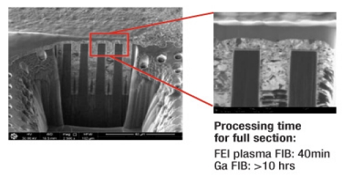
In a podcast interview, FEI product marketing manager Peter Carleson explained that gallium FIBs are already used for packaging applications, but with the cross-sections and trenches necessary for such applications (in the neighborhood of ~100µms), the removal process can take three, four, or even 8 hours. With the new source’s higher beam current, more samples can be done with greater tool utilization. The PFIB can also access lower regions of stacked dies to do traditional failure analysis or debugging (with the device "on") on the devices in the lower regions. The PFIB also enables quicker cross-sectioning of 3D integrated circuits that use TSVs/interposer layers (Fig. 2).
Click to Enlarge

Figure 2. High-speed sectioning of TSVs with plasma FIB. The device was located, cross-sectioned, polished, and imaged with PFIB. SOURCE: FEI

The product can perform site-specific removal of package and other materials to enable failure analysis and fault isolation on buried die; and circuit and package modifications to test design changes without repeating the fabrication process or creating new masks. Other applications include process monitoring and development at the package level, and defect analysis of packaged parts and MEMS devices.

Listen to the podcast:


  • Format: mp3
  • Length: 4:29
  • Size: 4.10 MB
  • Date: 06/13/11

POST A COMMENT

Easily post a comment below using your Linkedin, Twitter, Google or Facebook account. Comments won't automatically be posted to your social media accounts unless you select to share.

FEI plasma FIB tool suits MEMS, 3D packaging

By Debra Vogler, senior technical editor

June 13, 2011 — FEI launched its Vion plasma focused ion beam (PFIB) system based on inductively-coupled plasma (ICP) source technology using a xenon ion beam. The system generates more than a micro-amp of beam current and can remove material faster (>20× improvements in speed, Fig. 1) than liquid metal ion sources that typically max out at a few tens of nano-amps, according to the company. Because of its speed, FEI will target new technologies, such as 3D packaging and 3D transistor design technologies, where PFIB analysis is more practical.

Click to Enlarge
  • High-volume milling/high beam current
  • Ga-FIB loses size advantage to plasma source as beam current goes above 50-60 nA
  • Xe has high sputter yield, high brightness, and low energy spread
  • No Ga contamination

Figure 1. Plasma FIB is 20× faster than current FIBs. Its fast ion milling capabilities enable rapid cross-sectioning of features from 50-1000µms. SOURCE: FEI

In a podcast interview, FEI product marketing manager Peter Carleson explained that gallium FIBs are already used for packaging applications, but with the cross-sections and trenches necessary for such applications (in the neighborhood of ~100µms), the removal process can take three, four, or even 8 hours. With the new source’s higher beam current, more samples can be done with greater tool utilization. The PFIB can also access lower regions of stacked dies to do traditional failure analysis or debugging (with the device "on") on the devices in the lower regions. The PFIB also enables quicker cross-sectioning of 3D integrated circuits that use TSVs/interposer layers (Fig. 2).

Click to Enlarge

Figure 2. High-speed sectioning of TSVs with plasma FIB. The device was located, cross-sectioned, polished, and imaged with PFIB. SOURCE: FEI

The product can perform site-specific removal of package and other materials to enable failure analysis and fault isolation on buried die; and circuit and package modifications to test design changes without repeating the fabrication process or creating new masks. Other applications include process monitoring and development at the package level, and defect analysis of packaged parts and MEMS devices.

Listen to the podcast:


  • Format: mp3
  • Length: 4:29
  • Size: 4.10 MB
  • Date: 06/13/11

POST A COMMENT

Easily post a comment below using your Linkedin, Twitter, Google or Facebook account. Comments won't automatically be posted to your social media accounts unless you select to share.