June 13, 2011 – PRNewswire — IBM (NYSE: IBM) Research scientists have demonstrated an integrated circuit (IC) fabricated from wafer-scale graphene, creating a broadband frequency mixer operating at frequencies up to 10 gigahertz (10 billion cycles/second).
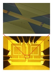
 IBM was able to integrate graphene transistors with other components on a single chip, overcoming past challenges like poor adhesion of graphene with metals and oxides and unreliable fabrication processses. The IC combines a graphene transistor and a pair of inductors on a silicon carbide (SiC) wafer, fabbed with wafer-scale processes that maintained graphene quality.
Graphene was synthesized by thermal annealing SiC wafers to form uniform graphene layers on the wafer surface. Four metal layers and two oxide layers formed the top-gated graphene transistor, on-chip inductors and interconnects. The fabrication method can be applied to other types of graphene materials, including chemical vapor deposited (CVD) graphene films synthesized on metal films, and is compatible with optical lithography.
In 2010, IBM developed an epitaxially grown graphene transistor with 100GHz cutoff frequency. IBM noted at the time that their research was focused on process technologies compatible with silicon device fabrication. Much like the device announced today, the graphene transistor was grown on SiC with a top-gate structure.
Today’s analog graphene-based IC is designed for wireless communications, improving cellular operation at conventional frequencies; and for use at much higher frequencies to replace X-rays for military (weapons screening) and medical personnel (medical imaging). The circuit is a broadband frequency mixer, which produces output signals with mixed frequencies of the input signals for communications systems.
Single-layer, lattice-structured graphene could use less energy and cost less than conventional silicon-based devices in portable electronics. Its electrical, optical, mechanical and thermal properties promise better and new performance abilities. The new device boasts thermal stability to 125°C and frequency mixing to 10GHz.
The breakthrough is shared between IBM and the Carbon Electronics for RF Applications (CERA) program, funded by DARPA.
The graphene-based IC is highlighted in Science: http://www.sciencemag.org/content/332/6035/1294.short
The Binnig and Rohrer Nanotechnology Center opened at IBM Research – Zurich in May 2011. Learn more at http://www.ibm.com

