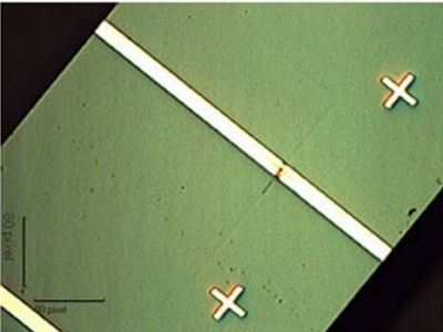
June 14, 2011 — Department of Electronic and Electrical Engineering at UCL and the London Centre for Nanotechnology researchers have demonstrated an electrically driven, quantum dot laser grown directly on a silicon (Si) substrate, with a 1300nm wavelength suitable for telecommunications electronics.

Silicon photonics — optical interconnects for use with silicon electronics — will enable electronics to handle larger quanitites of data than current copper interconnects. However, silicon has proven to have a difficult atomic structure for light sources. Semiconductor lasers provide high-efficiency, direct interfaces for silicon electronics and data modulation. Direct compound semiconductor laser material growth on silicon could spur silicon photonics. However, the crystal lattice constants differ significantly between silicon and compound semiconductors, causing dislocations in the crystal structure. This leads to low efficiency and short operating lifetime for semiconductor lasers.
The UCL group developed special layers to prevent dislocations from reaching the laser layer, and a quantum dot laser gain layer. They demonstrated the technique on an electrically pumped 1,300nm wavelength laser grown by direct epitaxy on silicon.
In a recent paper in Optics Express (Vol. 19 Issue 12, pp.11381-11386 (2011)) they report an optical output power of over 15mW/facet at room temperature.
In collaboration with device fabricators at EPSRC National Centre for III-V Technologies, the team demonstrated the first quantum dot laser on a germanium (Ge) substrate by direct epitaxial growth. The laser, reported in Nature Photonics , (DOI: 10.1038/NPHOTON.2011.120, 12 June 2011) is capable of continuous operation at temperatures up to 70C and has a continuous output power of over 25mW/facet.
Quantum dot gain layers improve tolerance to residual dislocations relative to conventional quantum well structures, said Dr Huiyun Liu, epitaxy research leader and Royal Society University Research Fellow in the UCL Department of Electronic and Electrical Engineering. "Our work on germanium should also permit practical lasers to be created on the Si/Ge substrates that are an important part of the roadmap for future silicon technology."
Future work will tackle combining the lasers with waveguides and drive electronics, furthering silicon photonics integration, added Professor Alwyn Seeds, Head of the Photonics Group in the UCL Department of Electronic and Electrical Engineering, Principal Investigator in the London Centre for Nanotechnology and Director of the EPSRC Centre for Doctoral Training in Photonic Systems Development.
Learn more at http://www.ucl.ac.uk/

