by Dr. Paula Doe, SEMI Emerging & Adjacent Markets
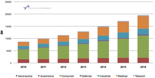
June 7, 2011 – Rapid growth in mainstream consumer markets is changing the structure of the MEMS industry from an artisanal to a volume manufacturing business. Yole Développement projects the MEMS market will near the $10 billion level this year, and is poised for 14% compound annual growth for the next five years, to approach close to $20 billion by 2016.
 |
| MEMS forecast per application. (Source: Yole Développement) |
These volume markets demand more efficient, non-artisanal solutions for moving designs into production. At the same time, with the maturing of the basic manufacturing technology, the value is moving from the device to the function and the system. And all these developments create a new set of challenges and opportunities to companies to find better ways to speed the ramp to low-cost volume production, to find better ways to integrate multiple die and software into easy-to-manufacture and easy-to-use functions, and to find the right business models to best use these skills to succeed.
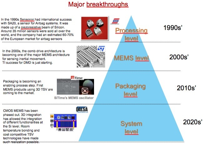
There has been a steady evolution over time, notes Yole founder and CEO Jean Christophe Eloy, as the young MEMS industry has matured to delivering higher functionality, from the manufacturing of MEMS structures in the 2000s, to the more recent innovations in integrated packaging. Coming next will be innovations in wafer bonding and through-silicon via (TSV) integration of multiple sensors and controls, requiring both packaging expertise for the integration and software expertise for managing the complex sensing and actions to be useful — raising the question of who in the value chain will do these steps.
 |
|
30 years of MEMS manufacturing history, an evolution aimed at climbing the value chain
toward increasing functionalities at the system level. (Source: Yole Développement) |
The demand for rapid ramp to high-volume production is driving manufacturers to focus increasingly on ways to more efficiently re-use established process stacks or technology platforms or even product platforms for the more efficient development of new products. And the need to reduce cost for consumer products is driving a relentless push to smaller die size, and to integration by TSV or wafer bonding when possible, and to solutions like capping the MEMS with the ASIC or making use of SOI to form the cavity, says Eloy.
GlobalFoundries’ Rakesh Kumar, director of MEMS, argues that there’s big potential to apply an IC foundry’s best known methods and practices — worked out after many years of experience in semiconductor tools and technologies — toward the more efficient manufacturing of MEMS. To be successful, an IC foundry must lower costs, offer high yield and high-performance MEMS products in a manner similar to ICs, while also shortening time-to-market by reduced technology transfer time and fast ramp to production, he says.
Specialty MEMS foundries are also developing solutions. Claude Jean, EVP/GM at Teledyne DALSA Semiconductor, suggests that the traditional MEMS approach of developing products first on lab equipment then porting over to manufacturing tools is too slow for fast ramp to yields and fast cost reduction. Instead, he highlights the advantages of doing the final rounds of development with an infrastructure closer to production tools.
IMEC’s Jo De Boeck, SVP of smart systems and energy technology, suggests that MEMS technology platforms are required, supported with a design environment consisting of a reference tool flow, corresponding models and design kits and a basic design IP library. Moreover, successful product innovation implementation will require co-developing software and hardware into optimal systems solutions.
We’ve invited these speakers representing leading companies from different viewpoints across the value chain — as well as ones from major IDM Robert Bosch and startup Sand9 — to discuss these key industry issues at SEMICON West, Tuesday, July 12 ("The Future of MEMS". Right afterwards, for a more hands-on look at the future of MEMS, the MEMS Industry Group presents a demo zone of next-generation MEMS sensors in action, demonstrated by MEMS folks who can give the inside scoop on how they work.
Tuesday afternoon also features a related program focusing on packaging issues for heterogeneous integration of MEMS and CMOS. Microsoft’s GM of packaging, quality and reliability, Raj Master, will give the technical keynote, followed by an update on market trends from TechSearch International and IHS iSuppli, and a panel discussion including Fraunhofer IZM, Toshiba Corp. and CEA-Leti, moderated by Analog Devices and NIST.

