
PRASAD BACHIRAJU, Rudolph Technologies, Inc., Wilmington, Mass.
As IC manufacturers adopt advanced packaging processes and heterogeneous, multi-chip integration schemes to feed ever-greater consumer demand for more computing power in smaller and smaller spaces, their supply chains have become increasingly complex. A fab-wide view of the process, not so long ago the holy grail of yield management systems, now seems quaintly inadequate. Critical processes that affect finished product yields now occur in different facilities running diverse processes at locations spread around the world. A packaged electronics module may combine microprocessors, memory, MEMS sensors and RF communications, all from different fabs and each with its own particular history. Optimizing yields from such a complicated supply chain requires access to individual component genealogy that includes detailed knowledge of process events, equipment malfunctions and operational parameters, and much more. The latest generation of yield optimization systems consolidates this data – tool deep and supply-chain wide – in a monolithic database, providing end-to-end, die-level traceability, from bare wafer to final module test. Specialized algorithms, designed for “big data” but based on intimate knowledge of semiconductor manufacturing processes, can find hidden correlations among parameters, events and conditions that guide engineers to the root causes of yield losses and ultimately deliver increased fab productivity, higher process yields, and more reliable products.
Proactive Yield Perfection
Proactive yield perfection (PYP) is a comprehensive systems-level approach to perfecting yield through detailed surveillance and sophisticated modeling that identifies actual or potential root causes of excursions and establishes monitoring mechanisms to anticipate and proactively address problems before they result in yield loss. PYP is a logical extension of long-standing yield management practices that comprehends the dispersal and growing complexity of the manufacturing process and combines information from conventional defect detection, yield analysis, automated process control, and fault detection and classification techniques. It addresses two major obstacles identified within the industry: providing access to data across the fab and supply chain and integrating that data into device-level genealogy. PYP’s ability to correct small problems early is increasingly valuable in a complex supply chain where each step represents a considerable additional investment and a flawed finished module results in the costly loss of multiple component devices.
PYP collects data in a single database that integrates vital product parameter data from every die at each step in the process with performance and condition data from all tools, factories and providers in the supply chain. It provides unprecedented visibility of the entire manufacturing process from design, through wafer fab, test, assembly and packaging. Consolidating the data in a single, internally consistent database eliminates the considerable time often consumed in simply locating and aligning data stored in disparate databases at multiple facilities, and allows analytical routines to find correlations among widely separated observations that are otherwise invisible (FIGURE 1).
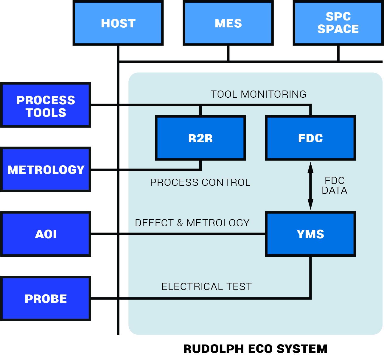
FIGURE 1. The PYP ecosystem
Genealogy incorporates traditional device-level traceability of every die, but also provides access to all information available from sensors on the tool (temperature, pressure), process events (e.g. lot-to-lot changes and queue times), equipment events (e.g. alarms and preventive maintenance), changes in process configurations (e.g. specifications and recipes), and any other event or condition captured in the database for sophisticated analysis. Ready access to device genealogy allows analysts to trace back from failed devices to find commonalities that identify root causes, and trace forward from causes and events to find other device at risk of failure.
Mobile communications
A leading global supplier of mobile communications products has implemented the full PYP suite across their supply chain (FIGURE 2), which includes three separately located front-end fabs, a fabless design facility, oursourced manufacturing (foundries), and outsourced assembly and test (OSAT). Finished modules integrate data processing, data storage, RF communications, power management, analog sensing, and other functions using multiple die and components fabricated at various facilities around the world. The PYP suite comprises fault detection and classification, yield management, defect detection and classification, and run-to-run automated process control, including configurable dashboard displays that provide interactive drill-down reports and scheduled user-definable reports. The process flow includes front-end wafer-based processing, with singulated die then transferred to tape and subsequently to rectangular panels for back-end processing (FIGURE 3).
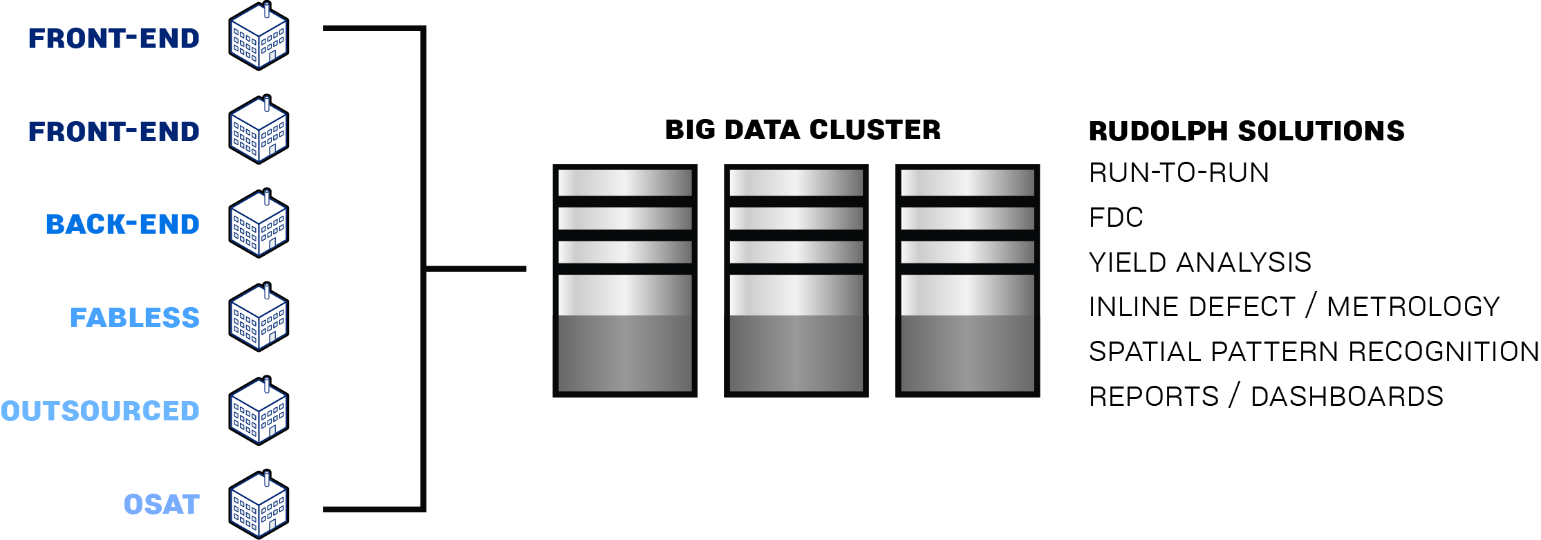
FIGURE 2. Numerous locations worldwide feed information into a single big-data cluster where multiple software solutions operate on the pre-aligned and internally consistent data set.
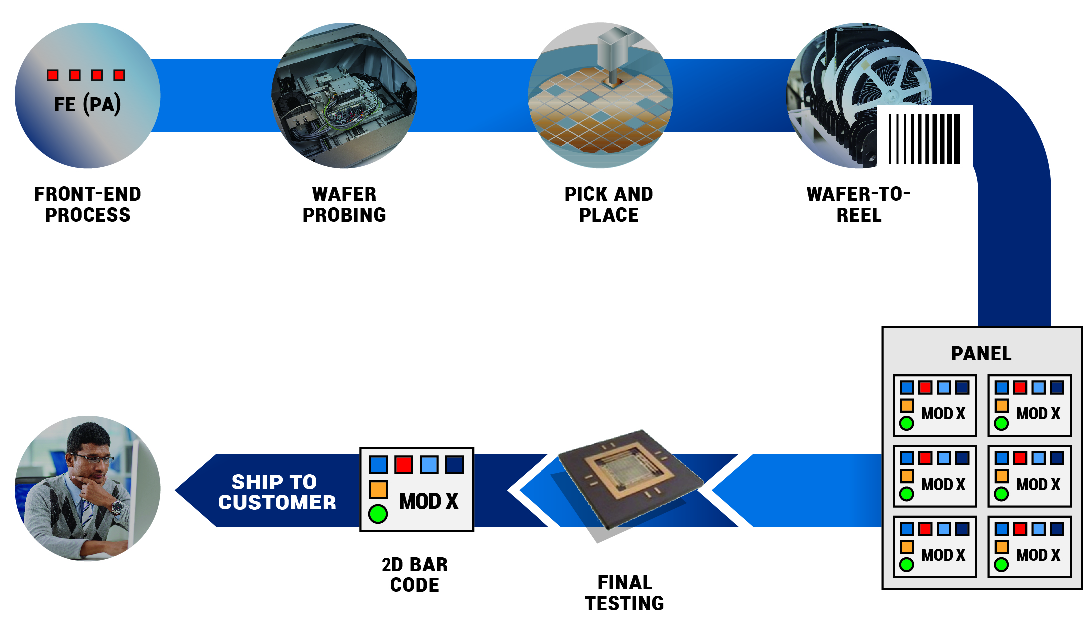
FIGURE 3. In a typical process flow, die move from wafer (front-end and back-end wafer fab), to reel, to panel, to final test and finally to the customer.
In one instance (FIGURE 4), panel mounted die were failing in back-end processing, causing yield losses valued at hundreds of thousands of dollars. The failed die were traced back to over a thousand wafers, and analysis of those wafers, using spatial pattern recognition, revealed defect clusters near the wafer edges. Further analysis of integrated MES (wafer process history) data traced the clusters to a defective tool that leaked etching solution onto wafers. Engineers are currently evaluating sensor data from the tool in an effort to identify a signal that will permit proactive intervention to prevent similar losses in the future.
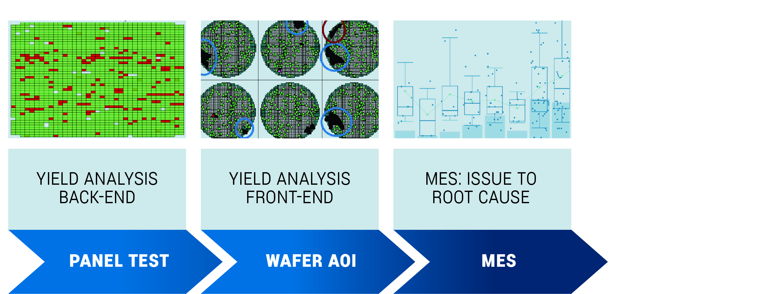
FIGURE 4. A potential loss of hundreds of thousands of dollars due to final test on panel (left) was traced back to over a thousand wafers. Through yield analysis, an SPR pattern signaled wafers with edge defect clusters (center). Finally, the root cause is understood through MES analysis (right).
In another case, failed die on panels in the back-end showed a characteristic “strip” signature (FIGURE 5). Tracing the die backward revealed a front-end a process issue with the failing die all originating from locations near the center of the wafer.
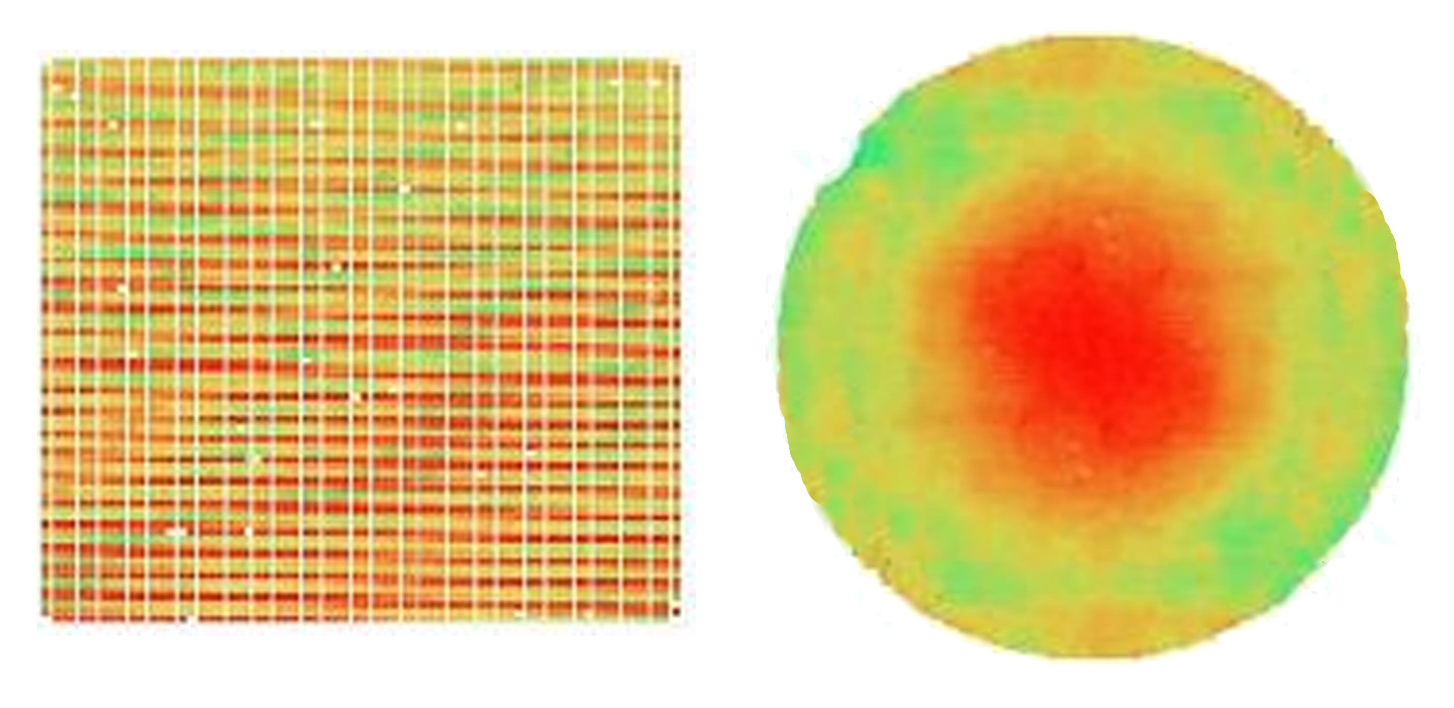
FIGURE 5. The bad die (red strips) on the panel (left) were traced back the centers of the original wafers.
A final example from this manufacturer occurred in the back-end where die containing various filter technologies fabricated on a wafers of different sizes are combined on a panel substrate (FIGURE 6). In this case, the customer gained additional insights regarding the origin of the die being assembled and was able to evaluate how shifts in performance parameters impacted the final module product. This resulted in better matching of parts in the pre-assembly process and a tighter distribution of performance parameters in the outgoing modules.

FIGURE 6. A single panel contains different filter components from multiple (differently-sized) wafers. Die-level traceability allows engineers to relate final test results to inspection and metrology data collected during wafer processing. Die can be traced back to their individual location on the original wafer, permitting associations with location-specific data such as defect patterns discovered by SPR.
Automotive electronics
A leading global supplier of electronic systems to the automotive market manufactures finished modules containing multiple ICs from various suppliers and facilities. Highest reliability with component failure rates at parts-per-billion levels is an absolute requirement because the health and safety of millions of drivers may be jeopardized by a defective product. Limiting these risks, and the associated financial liability, through fast root-cause analysis of in-house test failures and field returns and rapid identification of process drift or step function changes are critical needs. Tuning the process to improve yields while preserving critical reliability is an equally important economic concern.
The final product is a multi-chip module containing microelectromechanical system (MEMS)-based sensors from one supplier and application-specific integrated circuits (ASIC) from another. These component parts are functionally tested prior to being send to an assembly facility where they are attached to a common carrier and packaged in a sealed module, which is then retested to verify functionality of the completed assembly. PYP software collects data across the entire supply chain. Devices from a single wafer lot are ultimately split and mixed among many modules. Using a commonality analysis, engineers can quickly identify die that share a similar risk and track them to their ultimate dispositions in finished modules. The tracking is not limited to wafer level. For instance, it might be used to find only those die located on the straight-line extension of a known crack or within at-risk regions identified by spatial pattern recognition (SPR). Such information is critical in issuing a recall of at-risk parts.
In this case, die that were known-good at wafer test were failing after assembly. Tracing back to wafer level the customer determined that all affected modules were assembled within a short time period of one another. Further investigation found that the packaging process was affecting peak-to-peak voltage at final test. The customer was not able to modify the assembly process, but they were able to eliminate the final test losses by tuning wafer probe specifications to eliminate die at risk for damage in the assembly operation. Die-level traceability across the supply chain, which allowed engineers to quickly and easily compare data sets on the same dies from wafer probe and final test, was key to achieving this solution.
Conclusion
Increasingly dispersed and complex supply chains require a proactive, integrated, systems-level approach to optimizing yields. PYP’s ability to integrate data – sensor-deep and supply chain-wide – in a monolithic database streamlines analysis and finds relationships that are otherwise invisible. Die-level genealogy allows engineers to trace die histories backward to find root causes of failures and forward to identify other die similarly at-risk. The value of PYP-based solutions is multiplied by the substantial investments made at each step of the process and the high cost and potential financial liability associated with failed, multi-chip modules.
PRASAD BACHIRAJU is Director, Customer Solutions, Rudolph Technologies, Inc., Wilmington, Mass.
Editor’s Note: This article was originally published in the October 2018 issue of Solid State Technology.