by J. Braggin, Entegris, Billerica, MA USA (on assignment at IMEC); R. Gronheid, S. Cheng, D. Van Den Heuvel, S. Bernard, P. Foubert, IMEC, Leuven, Belgium; C. Rosslee, Sokudo Co. Ltd., Santa Clara, CA USA (on assignment at IMEC)
EXECUTIVE OVERVIEW
As Moore’s law drives the semiconductor manufacturing industry towards 32nm processing utilizing immersion lithography, microbridging defects have emerged as one of the top yield detractors. It is generally recognized that there are multiple root causes for microbridging defectivity, including image and resist contrast and different developer techniques, which have all been studied and described at length. In this study, we will focus on the effect of point-of-use filtration and how it is best used to mitigate microbridging defectivity.
December 18, 2009 – A design of experiment methodology will be utilized to understand the effect of various filter and filtration parameters on microbridging defectivity, including filter retention rating, filter media and design, filtration rate, and controlled filtration pressure. By better understanding the effect of point-of-use filtration on microbridging defectivity, guidelines for better control of this type of defect may be formulated.
Microbridging defects have been one of the most interesting and frustrating challenges facing lithographers for years, beginning with dry lithography [1] and moving into the immersion lithography era. As line widths shrink, the size of a killer microbridging defect also shrinks. It is with this challenge in mind that consumable suppliers, equipment and resist manufacturers work to find the root cause of microbridging defects and ultimately reduce or eliminate them.
Many root causes of microbridging defectivity have been previously identified. Image and resist contrast implications [2], polymer uniformity [3,4], developer contributions [3,5], BARC contributions [1], the location and size of particles and bubbles in immersion fluid [6,7], and resist manufacturing filtration [3,4] may all contribute to microbridging defectivity. No single root cause can completely explain the defect, nor be used to completely eliminate this defect. To reduce microbridging defects to acceptable levels, optimizing each contribution is required.
This study focuses on using point-of-use filtration on the lithography track to reduce the level of microbridging defectivity in a 45nm line/space pattern created through immersion lithography. A design of experiment methodology was used to determine the effect, if any, that filter retention rating, membrane material, filtration rate and controlled filtration pressure had on microbridging defectivity. This paper presents the results obtained in 2008 at IMEC. Additional results will be published at SPIE 2010.
Coating and exposure conditions
All wafers used for the microbridging project were coated and exposed on the Sokudo RF3S/ASML XT:1900Gi cluster. For all defect results, the Entegris IntelliGen Mini dispense system was used with Entegris Impact Mini resist filters. IMEC’s Defect 45 mask was used for the exposures. The Defect 45 mask is designed to print nine uniform sub-dies of 45nm lines with 90nm pitch.
The resist stack for this experiment consisted of 95nm ARC29SR and 105nm TOK TARF Pi6 001ME resist. A post-soak step was used after the exposure, and development was done with a slit-scan nozzle. The exposure conditions used for this study are NA = 1.35, Dipole40X, σi = 0.62 σo = 0.82 with y-polarization. A dose of 20mJ and focus = 0μm were used for all exposures.
Metrology setup
The initial phase of the study was to determine the best metrology recipe to detect the highest number of microbridging defects with the lowest number of nuisance defects.
To begin the metrology study, four wafers were exposed with the Defect 45 mask utilizing the IMEC process of record (POR) chemistry. These wafers were inspected with the baseline version of the IMEC POR KLA 2800 recipe, the parameters of which are shown in Table 1. During the scan of one wafer, sensitivity tuning was used to inspect the entire wafer with an aggressive threshold level. After the inspection, each defect was binned by the threshold level at which it had been detected.
 |
| Table 1. Experimental recipe conditions. |
Next, a subset of the smallest defects from each bin was reviewed with the AMAT SEMVision G3 STAR. It was determined through the review process that a suitable, sensitive recipe would require an optimized threshold. By changing the threshold value, the signal-to-noise ratio was optimized, thereby increasing the number of real, small defects of interest while having an acceptable, low level of nuisance defects.
Two additional recipes also were compared to this improved recipe to determine their effectiveness in finding microbridging defectivity. The different settings tested are recorded in Table 1. The first KLA 2800 recipe tested was based on an OEM’s standard recipe, which utilized the high performance edge contrast (HPEC) mode with a 0.2μm pixel. The combination of features on this recipe are similar to the IMEC POR recipe, but render it less sensitive to nuisance from vertical and horizontal structures.
The second KLA 2800 recipe was a high sensitivity brightfield inspection with a 0.08μm pixel size. This type of inspection has been traditionally used in fabricators utilizing KLA equipment. Wafers were inspected with all three tests to compare defectivity levels. On the whole, the defectivity levels across the different inspections were similar. The SEM review provided more information about the unique defects each recipe detected. The IMEC POR and HPEC recipes were quite comparable. Each recipe detected low levels of unique microbridging defects; however, when compared to the IMEC POR recipe, the majority of the added defects found by the brightfield recipe were SEM non-visible nuisance defects.
The final test to check the performance of the recipe was to run IMEC POR and HPEC recipes tuned specifically for a Defect 45 reticle with programmed microbridging defects of varying sizes. The IMEC POR recipe detected 1,000 more defects than the HPEC recipe, all of which were line protrusions, or small pieces of resist reaching across the space, but not reaching the next nearest neighboring line. Therefore, it was determined that this was the best recipe to continue utilizing.
Materials used
The POR version of the resist with the planned track, pump and filter setup was found to have too low a level of microbridging defects to show statistical significance between factors tested. Therefore, it was decided to increase the challenge concentration of microbridging defects by utilizing a special version of the TOK TARF Pi6 001ME resist. The version provided yielded 10 times the number of microbridging defects than the POR sample provided
Design of experiment
The experiment consisted of testing different Impact Mini filters and different user-defined filtration parameters on the IntelliGen Mini dispense system. The different factors available for the design of experiments are listed in Table 2. Two to three wafers were coated for each condition set.
 |
| Table 2. Experimental factors available for the design of experiments. |
Filtration parameters description
The IntelliGen Mini dispense system uses patented two-stage technology to completely separate dispense from filtration, creating a more accurate and repeatable dispense without being concerned with the effect on the point-of-use (POU) filter’s ability to filter the material. The separation of these two functions allows for tighter and more direct control of filtration parameters when utilizing the most advanced POU filters. Filtration pressure for this study is defined as the pressure applied to the filtrate once it has passed through the filter membrane. Filtration rate is defined as the rate at which the motor in the first chamber pushes the chemistry through the membrane.
Experimental procedure
All wafers used in this study are scanned with a KLA SP2 recipe prior to coating. For each filter set, the filter to be used is primed on the IntelliGen Mini in advance. All wafers for each filter set are coated utilizing the same filter within a two-day timeframe.
KLA 2800 inspections take place as soon after the exposure as possible. KLA 2800 results are compared to SP2 results to remove prior level defects that are not of interest in this study. In addition, hot spots and large clusters with known root cause defects are removed from the review sample in order to study random defectivity. Because of limited availability of the review SEM, in cases when too many defects are present on the wafer, a reasonable sample of defects were chosen.
All SEM review was performed by the same person utilizing only the top-down images to ensure classification accuracy. Minitab 15 was used to generate the box plots and main effects plots and was used for the analysis of the design of experiments.
Results
All results presented represent current-level resist defects, as prior-level bare wafer defects have been removed from the review sample. Reported defects are directly related to POU filter performance and microbridging defectivity. Additional defects were detected, but are not reported in this study.
The results of the 2008 defect studies are seen in Figure 1 and Figure 2. Microbridging is the largest contributor to defectivity in the defect groups shown.
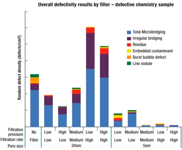 |
| Figure 1. All defective chemistry results with varying filtration rate and pressure. N/A indicates that a flushing shell was used for preliminary data collection. |
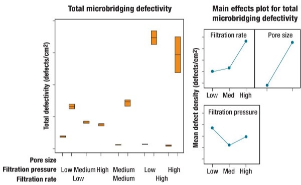 |
| Figure 2. All defective chemistry results for total microbridging defectivity with varying filtration rate and pressure. |
When comparing all the data, it was determined that filter pore size is statistically significant for reducing microbridging defects, whereas filtration rate and pressure are not. It is hypothesized that this is due to the different designs of the filter membrane tested, particularly symmetry. When analyzing the filter results separately, different results are obtained.
20nm symmetric UPE results. Initial 20nm symmetric UPE results were obtained over two days of experiments. The results, shown in Figure 3 and Figure 4, demonstrate the effect of filtration rate and pressure on overall microbridging defectivity. As has been discussed in other studies previously [8], lower filtration rates have a positive effect on overall defect density and yield. This is true in this study as well, where the low filtration rate gave statistically significant better results than the high filtration rate. This phenomenon is likely due to microbubble generation in the symmetric filter when trying to filter the chemistry at too fast a rate. The high filtration rate may shear the resist, and thus cause outgassing of the resist leading to bubbles in the dispense line, which ultimately create defects on the wafer. Although filtration pressure was not a statistically significant factor in this filter study, a higher filtration pressure, when combined with a low filtration rate, provided the best overall defectivity results.
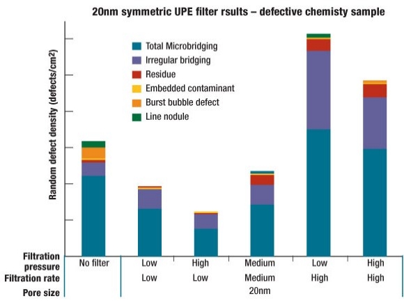 |
| Figure 3. 20nm symmetric UPE filter results with defective chemistry set and varying filtration rate and pressure. |
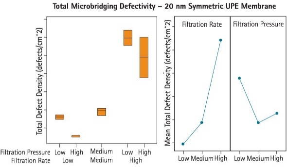 |
| Figure 4. 20nm symmetric UPE filter results with defective chemistry set and varying filtration rate and pressure. |
5nm asymmetric UPE results. Initial 5nm symmetric UPE results were also obtained over two days of experiments. The results, shown in Figure 5 and Figure 6, tell a different story than the 20nm symmetric UPE results. Within this data set, both filtration pressure and filtration rate were statistically significant contributors to microbridging levels, with a high rate and pressure combination providing the best results.
It is hypothesized that this result is due to the filter’s pore size and membrane design, specifically its asymmetry. The asymmetric design provides an improved flow rate, the ability to utilize more membrane surface area, and an increase in chemistry residence time in the porous structure. As the chemistry is being quickly filtered through the membrane, it is hypothesized that potential microbridging defects are broken apart, and thus do not appear in the exposed pattern. However, if the filtration rate is lowered, the components creating the microbridging defect may be able to continue through the membrane.
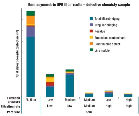 |
| Figure 5. 5nm asymmetric UPE filter results with defective chemistry set and varying filtration rate and pressure. |
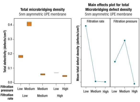 |
| Figure 6. 5nm asymmetric UPE filter results with defective chemistry set and varying filtration rate and pressure. |
Conclusion
Microbridging defectivity has many root causes, and no one approach can be used to completely eliminate this defect mode; however, this study demonstrated that simply decreasing point-of-use filter pore size can reduce overall defectivity, and more specifically microbridging defectively. In addition to this fairly simple change, optimizing filter-specific dispense system parameters can further reduce microbridging defectivity.
Acknowledgments
The authors would like to thank TOK for providing the special sample of resist used in this study. The authors would also like to thank G. Marcuccilli (KLA-Tencor) and T. Batchelder, P. Magoon, R. Ramirez, and A. Wu (Entegris, Inc.) for useful discussions and support.
IntelliGen, Impact, and Minitab are registered trademarks of Entegris.
References
[1]. M. Randall, et al., "Minimizing Wafer Defectivity During High Temperature Baking of Organic Films in 193nm Lithography," Proc. SPIE, 6153, 31 (2006).
[2]. B. Rathsack, et al., "Image Contrast Contributions to Immersion Lithography Defect Formation and Process Yield," Proc. SPIE, 6924, 18, (2008).
[3]. M. Kim, et al., "The Study of Defect Control and Patterning Performance for Top Coating Free Resist Process," Proc. SPIE, 6293, 69, (2008).
[4]. S.G. Chon, et al., "Improvement of Defect Issues for Advanced 193nm Resist," J. Photopolymer Science and Technology, 17 (4), 545-548 (2004).
[5]. S. Wu, et al., "Non-topcoat Resist Design for Immersion Process at 32nm Node," Proc. SPIE, 6923, 6, (2008).
[6]. P. De Bisschop, A. Erdmann, A. Rathsfeld, "Simulation of the Effect of a Resist-surface Bound Air Bubble on Imaging in Immersion Lithography," Proc. SPIE, 5754, 24 (2005).
[7]. M. Beyer, et al., "Production Aspects of 45nm Immersion Lithography Defect Monitoring using Laser DUV Inspection Methodology," Proc. SPIE, 6922, 04 (2008).
[8]. P. Do, et al., "Optimized Dispense Recipes for 20nm Filtration for Reducing Resist Defects," Solid State Technology, June (2004).
Biographies
Jennifer Braggin received her MS in engineering science from Rensselaer Polytechnic Institute and her BS degree in materials science and engineering from Lehigh U. and is the dispense products applications engineer at Entegris, Inc., 129 Concord Road, Billerica, MA 01821 USA; e-mail [email protected].
Roel Gronheid received his PhD from Leiden University at IMEC and is a scientist in charge of resist fundamentals research in the lithography department at IMEC, vzw, Kapeldreef 75, B-3001, Leuven, Belgium.
Dieter Van Den Heuvel is process engineer of lithography at IMEC.
Sophie Bernard received her PhD in polymer chemistry from the University of Florida and is Entegris’ industrial assignee to IMEC.
Philippe Foubert received his PhD in chemistry at the University of Leuven and is R&D engineer in the lithography department at IMEC.
C. Rosslee is currently on assignment at IMEC, and is at Sokudo Co. Ltd., 3303 Scott Blvd., Santa Clara, CA 95952 USA.

