by Debra Vogler, senior technical editor, and James Montgomery, news editor, Solid State Technology
December 1, 2009 – Applied Materials is making a splash at this year’s SEMICON Japan with the release of three new tools: a dual-wafer CMP platform, a system for NiSi contact-layer annealing, and an integrated abatement/pumping system for emissions control.
Doubling down with dual-wafer CMP platform
Tackling the cost of consumables as well as productivity, Applied’s new Reflexion GT CMP platform targets copper interconnect planarization as well as tungsten applications. The company says the tool is production-ready for 4Xnm applications and beyond; there are also several beta units at both logic and memory end users, with processes being studied at 4Xnm and below.
The system has twice the pad life with up to 30% less slurry usage, according to Sidney Huey, GPM manager of Applied’s CMP division. However, a significant factor in achieving the system’s productivity gain in throughput — 80wph for a 30k logic or 120k memory WSPM scenario (with 6kÅ incoming copper) — is a dual-wafer architecture. This dual-mode scheme enables two wafers to be processed simultaneously on each platen, with the polishing heads independently controlled.
A shield around each platen works in concert with an exhaust system to handle misting/aerosols, etc., Lakshmanan Karuppiah, VP/GM of Applied’s CMP division, told SST. He noted that the shield design was improved from previous iterations to enable the two wafers/pad design and the faster system speed of the new tool. Furthermore, the ratio of the pad surface (each pad is 42in.) and pad conditioning ensures on-wafer performance is not compromised. Karuppiah noted that the much larger pads used in this design are essential; "they are double the surface area of pads used in a single-wafer tool (30in. pad)," he said.
Additionally, the design incorporates dedicated slurry and pad conditioning arms, critical to providing consistent performance, Huey told SST. "Having dedicated arms and slurry delivery and pad conditioning for each head allows polishing left and right sides and achieving matching performance."
Annealing for sensitive NiSi contact layers
Targeting millisecond annealing required for creating the sensitive nickel silicide (NiSi) transistor contact layers in 45nm and beyond logic chips is Applied Materials’ Vantage Astra system.
Key factors in obtaining the ideal time-temperature profile for optimal Ni Si are: a low enough pre-heat to avoid uncontrolled diffusion, a "jump" temperature that is high enough to enable optimal activation without wafer breakage or agglomeration, and a dwell time that must be short enough to avoid wafer bowing and breakage, according to Jeremy Zelenko, global product marketing manager at Applied’s MDP/FEP business unit.
The dynamic surface annealing (DSA) system uses a compact diode-stack laser that scans across the wafer in a series of passes — heating the surface directly below the beam to a depth of 100μm. Because the bulk of the wafer acts as a heat sink, the very small portion of the wafer that was heated by the laser cools rapidly as the beam moves onto the next segment. The result, Zalenko told SST, is sub-millisecond exposure that allows for a very high maximum peak temperature, thereby enabling effective phase transformation or dopant activation. Modifying the scan speed determines the anneal dwell time.
The system uses a solid-state laser (therefore, no gas) and the optics and the laser itself are in a compact tube. According to Zalenko, the laser’s lifetime is at least two years and no maintenance is required throughout its lifetime. Additionally, "It’s so compact, that instead of moving the wafer, we move the laser back and forth," Zalenko told SST. "And we can have two chambers per system." End users can have whatever combination they want; e.g., two millisecond chambers, or a hybrid that combines a spike chamber and a millisecond chamber, etc. "From a COO perspective, it’s extremely beneficial," he said. Company data indicates a throughput of >40wph per two-chamber system.
Applied says that the silicidation achieved with its new system enables up to 5% greater device speeds and up to 15× lower leakage. According to Zalenko, the system is extendible to high-k/metal gate applications.
Emission control for CVD, etch tools saves 20% utility costs
The third tool being released by Applied this week aims to help semiconductor fabs significantly improve energy conservation and lower utility cost for abatement and vacuum pumping on process tools by >20%.
The iSYS platform installs in less than a day on a wafer processing tool, to sense real-time changes in the process chamber and direct subsystems into predefined standby states. Built-in sensors and software enable remote monitoring of cumulative energy savings and tracking energy-sustainability progress.
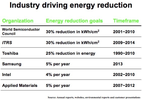
Corralling energy usage is of major and increasing interest to semiconductor manufacturers, Applied notes; industry bodies cite targets of 30% energy reduction over the past decade, with similar benchmarks laid out by individual chipmakers (see table below).

"By modulating resource consumption in response to changing tool conditions, the iSYS platform can help our customers lower their operating costs and support sustainable manufacturing practices," said Charlie Pappis, VP/GM of Applied Global Services, in a statement.
In tests at its Maydan Technology Center, the company says hooking the iSYS up to its Producer GT PECVD system using SEMI S23 methodology measured energy savings (power, water, and gas consumption) equivalent to 200MWh, or 220K pounds of CO2 emissions. The iSYS initially targets AMAT’s CVD tools, but can also support etch applications, the company notes.

