by Dwayne LaBrake, Zhengmao Ye, Cindy Brooks, Chris Jones, Frank Xu, Molecular Imprints Inc.
EXECUTIVE OVERVIEW
Up to now, the hard-disk drive (HDD) and semiconductor industries have utilized increasingly expensive exposure tools and complex lithographic processes to meet their technology roadmaps for higher density and performance at lower bit costs. Critical dimensions for both thin film heads and semiconductors have been shrinking at an accelerated rate. Now, with the addition of patterned media to the HDD technology roadmap, the resolution and cost challenges of the HDD industry are, in many ways, more challenging than those in the semiconductor industry. Critical dimension reductions forecasted for patterned media over the next decade are faster than NAND flash memory — the most aggressive of the semiconductor lithography roadmaps. To maintain ~40% per year growth in areal density to well beyond one terabyte/in2 will require patterned media with critical dimensions under 20nm, at less than one-tenth the cost of current semiconductor patterning.
Perpendicular magnetic recording (PMR) based HDDs are nearing the end of their technical capability for maximum storage density [1-3]. In anticipation, a new approach is being developed, called patterned media (PM), which is expected to take HDD media well beyond 1TB/in2. To produce PM, magnetic media is physically patterned using imprint lithography. The first incarnation of PM will be discrete track media (DTM) that will separate the data tracks in one dimension with lines and spaces. The ultimate incarnation of PM, called bit patterned media (BPM), will separate the data bits in two dimensions with individual bits as pillars [4,5]. PM marks a significant paradigm shift for disk media manufacturing with the introduction of high-resolution lithography processes at feature sizes and pitches that rival those used in semiconductor chip manufacturing.
The cost and resolution challenges facing HDD manufacturers as they transition to PM require adoption of a new lithography technology, since existing approaches developed for semiconductor companies are simply incompatible on a cost and throughput basis with the HDD industry’s roadmap. Jet-and-flash imprint lithography (J-FIL), which uses targeted inkjet drop dispensing of UV curable resist to print extremely small features on substrates down to below 20nm, has demonstrated the ability to meet the resolution, throughput and cost requirements for DTM and BPM applications.
This article provides an overview of the patterned media manufacturing process flow and how it fits in the current disk media manufacturing flow. J-FIL technology and its benefits for patterning media in manufacturing will also be reviewed. For successful manufacturing of DTM and BPM patterned media, high-throughput double-sided imprinting and low-cost imprint masks are required. As a result, the fabrication of master imprint templates, the replication of these to create working imprint templates, and imprint performance data from patterning disks using a double-sided imprint technique will also be covered.
Patterned media manufacturing
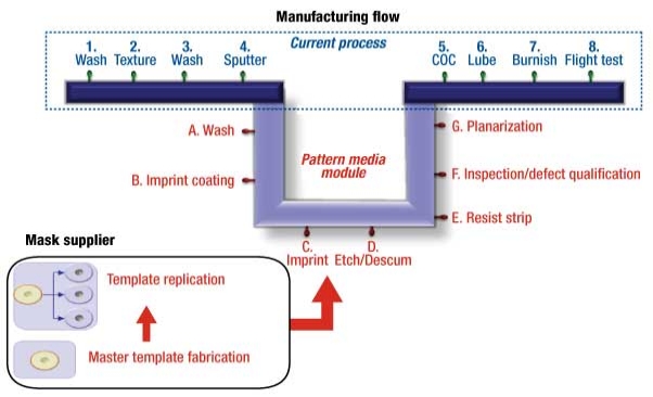
The current disk fabrication processes are outlined in Figure 1. They include disk washing followed by sputter coating of the necessary PMR film stack, including an anticorrosion diamond-like carbon (DLC) film. Subsequent application of a lubricant followed by burnishing and finally fly testing encompasses the main steps necessary for fabrication of PMR HDD media. Today, the manufacturing lines used to fabricate these disks require a relatively clean environment and can produce more than 1000 disks per hour (dph). The current manufacturing processes have been in place for many years and relatively few changes in the process steps and equipment were necessary to make the transition from longitudinal recording media to PMR.
 |
| Figure 1. Schematic of the hard disk manufacturing process, including patterned media. The dark blue bar represents process steps for present day perpendicular recording media, while the light blue bar represents process steps to be added for patterned media. Additional steps for template fabrication are noted at lower left. |
With the introduction of PM, a new set of process equipment and process steps are required. When fully introduced in manufacturing, PM will require additional steps including a sputtered disk cleaning step, followed by application of a vapor phase imprint adhesion layer, imprint patterning, reactive ion etching of the imprinted residual layer, pattern transfer of the magnetic film stack, resist strip, disk cleaning, and finally planarization of the patterned media. These new steps will be inserted into existing process as depicted in Fig. 1 and will require new manufacturing systems and extensive process development. These systems and processes will in turn require new skills of manufacturing engineers to successfully implement PM manufacturing.
Of all the technologies, J-FIL is new to lithographic manufacturing. This new type of lithography requires new infrastructure such as high-speed double-sided imprint process modules, the fabrication and low-cost replication of master templates, high-throughput vapor adhesion materials and systems, and imprint materials suited for high-throughput, low-defectivity imprint patterning.
Template fabrication
A supply of low-cost, precision templates is critical to high-volume, low-cost PM manufacturing. To accomplish this, a J-FIL based, high-volume template replication system is being developed. The system uses master templates that are fabricated using conventional e-beam and mask fabrication techniques in synthetic quartz [6]. The principle difference between conventional photomasks and templates used for HDD is that a rotary e-beam tool is required to pattern the ~500μm thick and 150mm diameter synthetic quartz substrates. Rotary e-beam systems have been developed with the necessary accuracy to meet the demands of disk drives where the data track line width variation is ~10% of the track pitch. Currently, the e-beam write time for a template to pattern a 65mm diameter disk with ~80nm pitch data tracks is 5-6 days. Such long write times result in very costly master templates so that template replication is required to meet cost-of-ownership (CoO) targets.
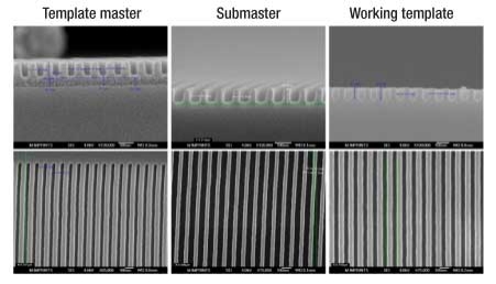
Using the replication system, the replica template is fabricated with the opposite tone of the master template so that the disk pattern tone matches that of the master template. This ensures critical areas of the disk surface are protected by imprint resist during pattern transfer. The basic process flow includes specialized cleaning processes to ensure no front- and back-side particle contamination of the blank replica substrate, followed by spin-on adhesion layer, imprinting this substrate using the master template, reactive ion etching of the residual layer, hard mask and synthetic quartz substrate and finally hard mask stripping and cleaning of the new template [7]. This process flow has been demonstrated for template features of <35nm. Figure 2 schematically depicts the process sequence and results for 100nm pitch DTM replication. Having a supply of low-cost working templates is a key part of the manufacturing strategy of HDD companies and is enabled by the J-FIL process.
 |
| Figure 2. SEM micrographs taken of imprint of the master template (left), a submaster (middle) and the working replica (right). The features are 100nm pitch. Note the duty cycle differences between the master, submaster and replica. |
Disk imprinting and materials
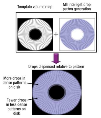
The J-FIL HDD process involves three key elements: an imprint system, templates and imprint materials (i.e., anti-adhesion and adhesion layers, and imprint resists) [8,9]. J-FIL uses a drop-on-demand inkjet resist dispense driven by the IntelliJet system to deliver pico-liter-sized resist droplets to the disk in a spatially selective manner such that the dispensed resist volume is distributed to match that of the template spatial volume distribution. The customized drop pattern is generated by proprietary algorithms upon which the drop generation software is based. This ensures that the local dispensed resist volume matches that of the template such that after imprinting, the residual layer is extraordinarily thin (typically <15nm) and uniform. Figure 3 depicts the sequence of drop generation and the residual layer uniformity in the presence of pattern density variations on standard DTM patterns. As shown in Figure 4, the 15nm target residual layer thickness (RLT) is met in both the data and servo regions.
 |
| Figure 3. Steps required to making a drop pattern using the IntelliJet drop pattern generator. First the volume map is calculated. Using the volume map, IntelliJet calculates the required drop pattern density to ensure volume matching of the imprint resist to the template pattern. The resulting drop pattern is then provided to the imprint tool for imprinting. |
The J-FIL process has several advantages over conventional spin-on resist coating methods, including, but not limited to: 1) low-volume usage of ~150 nanoliters per disk surface; 2) no edge bead removal required at the disk inside diameter or outside diameter; 3) ability to match the resist volume to the template in a spatially selective manner thus enabling very uniform RLT; 4) low capital equipment cost since costly spin coater tool is required; and 5) no resist waste stream disposal or solvent reclaim problems. The throughput of a current-generation HD2200 imprint system is >150dph and the next-generation high-volume manufacturing system will run at 360dph, so 2-3 systems would serve a 700-1000dph disk manufacturing line. In order to implement imprint in a manufacturing environment, the template and resist system must be capable of completing some 5000 imprints at low defectivity [10]. Several key aspects that have been pioneered to enable this include: 1) good wetting of the liquid imprint resist on the template and disk surfaces, which enables rapid filling of the template features for high throughput; and 2) anti-adhesion of the cured resist material to the template and high adhesion of the imprint resist to the disk substrate.
 |
|
| Figure 4. Example regions of an imprinted disk are shown in the above SEM images demonstrating that although the pattern density varies the residual layer thickness is uniform at 15nm. |
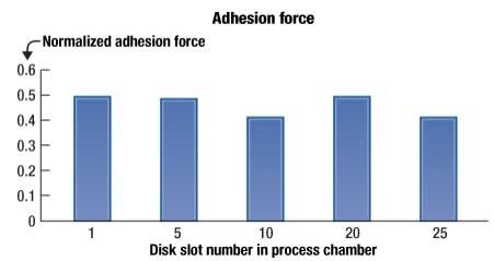
Because these capabilities may not be available at a single equipment supplier, cooperation among suppliers will be necessary to provide the required infrastructure in a timely manner. An example of this is the commercialization of ValMat, a vapor deposited adhesion promoter, which is applied using Intevac’s LithoPrime tool. As shown in Figure 5, the adhesion of a Valmat-coated surface to the imprint resist is sufficient to enable thousands of imprints to be made using a single template with very low defectivity. This, coupled with high throughput, low-material consumption, very thin and uniform films, and low CoO, make ValMat ideal for high-volume manufacturing.
 |
| Figure 5. A graph of normalized adhesion force vs. disk number in a 25-disk cassette, which demonstrates the superior adhesion of the imprint resist to a disk substrate when Valmat is used as the adhesion layer. |
Finally, Molecular Imprints has demonstrated pattern transfer using its imprint resists in conventional hard mask materials such as Cr, oxides and nitrides of Si and Ta, to name a few. The etch rate in appropriate hard mask etch processes of these imprint resists is similar to standard 193nm deep UV resists used in the semiconductor industry.
Conclusion
The addition of PM to HDD disk fabrication presents a number of new challenges to magnetic media manufacturers. J-FIL systems and materials for patterning magnetic media and template replication provide the foundation for successful high-volume manufacturing. The availability of low-cost templates from commercial photomask suppliers provides yet another key ingredient. Finally, we are working with deposition and etch equipment suppliers to help insure full process integration.
Acknowledgment
Jet and Flash, J-FIL and IntelliJet are trademarks of Molecular Imprints Inc.
Biographies
Dwayne LaBrake received his PhD in physical chemistry at Loyola U. of Chicago and is VP of applications and process integration at Molecular Imprints Inc., 1807 Braker Lane, Austin TX 78758; ph.: 512.339.7760; e-mail [email protected].
Zhengmao Ye received his PhD in electrical engineering at the U. of Texas at Austin and is hard disk drive applications manager at Molecular Imprints Inc.
Cindy Brooks received her PhD in plasma physics at the U. of Michigan at Ann Arbor and is template replication manager at Molecular Imprints Inc.
Chris Jones received his MS in chemistry at the U. of Texas at Austin and is senior applications engineer at Molecular Imprints Inc.
Frank Xu received his PhD in materials science at the U. of Massachusetts at Amherst and is director of materials technology at Molecular Imprints Inc.
References
1. D. Weller, M. F. Doerner, "Extremely High-density Longitudinal Magnetic Recording Media," Annual Rev. of Materials Science, vol. 30, pp. 611-644 (2000).
2. B. M. Chen, T. H. Lee, K. Peng, V. Venkataramanan, Hard Disk Drive Servo Systems, 2nd ed. (Springer, NY, 2007).
3. T. Oikawa, M. Nakamura, H. Uwazumi, T. Shimatsu, H. Muraoka, Y. Nakamura, "Microstructure and Magnetic Properties of CoPtCrSiO2 Perpendicular Recording Media," IEEE Trans. Magn., vol. 38, pp. 1976-1978 (2002).
4. S. Y. Chou, "Patterned Magnetic Nanostructures and Quantized Magnetic Disks," Proc., IEEE, vol. 85, no. 4, pp. 652-671 (1997).
5. C. A. Ross, "Patterned magnetic recording media," Annual Review of Materials Research, vol. 31, pp. 203-235 (2001).
6. D. J. Resnick, W. J. Dauksher, D. P. Mancini, K. J. Nordquist, E. S. Ainley, K. A. Gehoski, et al., "High-resolution Templates for Step and Flash Imprint Lithography," Jour. of Microlithography, Microfabrication, and Microsystems, Vol. 1, pp. 284-289 (2002).
7. M. Miller, G. M. Schmid, G. F. Doyle, E. D. Thompson, D. J. Resnick, "Template Replication for Full-wafer Imprint Lithography," Microelectronic Eng., vol. 84, pp. 885-890 (2007).
8. M. Colburn, S. C. Johnson, M. D. Stewart, S. Damle, T. C. Bailey, B. J. Choi, et al., "Step and Flash Imprint Lithography: a New Approach to High-resolution Patterning," Proc. SPIE – Emerg. Lith. Tech., vol. 3676, pp. 379-389 (1999).
9. M. Miller, C. Brooks, D. Lentz, G. Doyle, D. J. Resnick, D. LaBrake, "Step and Flash Imprint Process Integration Techniques for Photonic Crystal Patterning: Template Replication through Wafer Patterning Irrespective of Tone," Proc. SPIE, vol. 6883 (2008).
10. Preliminary experiments have demonstrated template lifetimes exceeding 104 imprints (unpublished data).

