by Ron Kool, ASML
March 7, 2011 – Extreme ultraviolet (EUV) lithography was one of six conference tracks and a major point of discussion at the 2011 SPIE Advanced Lithography symposium (Feb. 28-Mar.3, San Jose, CA), with dozens of papers presented on various technology and infrastructure areas of EUV development. EUV is generally considered the technology needed to extend the lithography roadmap; ASML believes EUV is the most economically viable, most extendible lithography technology for the 22nm node and beyond.
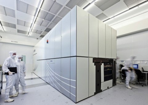
Progress made on ASML’s NXE:3100 pre-production system center on imaging and overlay potential to support the development work of chipmakers. Resolutions down to 18nm and 7nm matched machine overlay (MMO) were shown. Samsung, which received the first NXE:3100 system last fall and exposed wafers before the end of 2010, showed 27nm images exposed on the NXE:3100 using conventional illumination. IMEC has now received and begun installation of the second NXE:3100, and officially moves their EUV litho research program to the preproduction stage, shifting focus from mainly an infrastructure study to include a manufacturability study. Hynix also showed NXE:3100 exposures comparing a thick and a thin absorber reticle, including 22nm lines and spaces using dipole illumination.

Several chipmakers presented updates and analysis that indicated EUV litho provides the most advantageous roadmap. Toshiba addressed the comparison between quadruple patterning, single-exposure EUV, and double-patterning EUV techniques using the parameters of litho performance, process costs, and turn-around time. Their conclusion: EUV is the preferred technology for lowest cost-of-ownership and turn-around time, provided projected throughput targets are met. In general, >100 wafers per hour (wph) EUV is cost-effective relative to almost all other patterning schemes, and 125wph makes it cost-effective relative to all schemes.
Source power
Meeting these throughput targets depends on significantly increasing EUV source power, which although not the only challenge facing EUV, is its biggest hurdle to high-volume manufacturing (HVM) production. The first part of the challenge is getting to 60wph on ASML’s six NXE:3100 pre-production systems (two have already shipped to customers, and the remaining four systems will ship by mid-year). There are two pieces of good news regarding source power. First significant progress has been made, including a 20× increase in productivity, since the first EUV alpha demo tools (ADT) were shipped in 2006 (to IMEC in Europe and CNSE in the US). Second, all three source suppliers (Cymer, Ushio, and Gigaphoton) presented progress updates and roadmaps, showing they have developed platforms for their sources and have defined improvements to increase the power levels to achieve the targeted 60wph by end of this year. In addition, Cymer and Ushio have coupled sources to ASML NXE:3100 systems that have shipped to end customers.
Masks and resists
In addition to source power, two key areas of EUV infrastructure development that are instrumental to make EUV viable for HVM are blank and mask inspection and photoresists. Papers/presentations at SPIE 2011 showed a lot of solid work and progress on both fronts.
Progress was shown in the inspection and repair field, stimulated by US and Japanese programs, SEMATECH and EUVA. KLA-Tencor updated its blank and mask inspection roadmaps going down to resolutions of 8nm logic or 11nm memory, extending beyond optical inspection, using actinic wavelength. Zeiss showed that its AIMS tool development for mask repair is nearing the end of the concept phase and preparing to enter the development phase. Also, several papers were given on mask cleanability with good results, showing the broad scope of the mask work being done to support EUV litho.
On the resist front, the growing availability of exposure tools (six NXE:3100 systems installed by mid-year) will continue to enable the development of resists that began with the ADTs four years ago. This year’s SPIE saw papers showing resolution improvements, linewidth roughness control, and dealing with out-of-band radiation. Inorganic resists made significant progress in resolution down to 15nm, and at the same time dose improvements were reported — this year’s champion data from Inpria showed dose improvement already down to 25mJ/cm2 for 22nm dense lines, vs. ~100mJ/cm2 at SPIE 2010.
Other NGL
EUV is not the only next-generation lithography (NGL) technology — several papers and presentations at SPIE covered nanoimprint lithography (NIL), maskless e-beam, and self-assembly technologies.
The key challenges of NIL are low throughput, overlay, and defectivity. Progress was reported notably on defectivity and throughput performance — to the level of claiming to be entering acceptable performance for Toshiba. However, in a presentation that showed the options for their 1xnm arena, Toshiba did not mention nano-imprint in their candidates for HVM, and solely focused on double-patterning extension and EUV.
Progress on e-beam seems slow, with throughput remaining a significant hurdle. The impression from the papers presented is that overlay is also an area where large progress is needed, certainly in combination with the increasingly more aggressive targeted insertion point of the technology.
Good progress was shown on self-assembly techniques. Whereas NIL and e-beam can be considered market niches, and complimentary for instance in double patterning schemes, self-assembly will most likely be used in combination with other litho technologies and will be used as complimentary technology.
Conclusion
While EUV is not yet ready for manufacturing, progress is being made, roadmaps are in place and industry infrastructure is coming together. ASML expects that this progress will continue at an increased rate as NXE:3100 pre-production systems continue entering the market providing platforms for continued development.
Ron Kool is VP of ASML’s EUV product group.

