by Laura Peters, contributing editor
January 12, 2010 – The year 2010 is an even-numbered year, so the update to the International Technology Roadmap for Semiconductors (ITRS) generally undergoes few changes, saving the major changes for odd-numbered years. Nevertheless, substantial changes have occurred in 2010, including boosts in the timelines for NAND flash and DRAM device rollouts, backup plans for lithography forced by EUV delay, impending device and interconnect structural changes, and progress in 3D packaging.
The 2010 ITRS executive summary [PDF link] does an excellent job of highlighting the changes from 2010-2024 by chapter. Following is a much more abbreviated version of the top processing highlights.
Process integration, devices and structures
When the roadmap committee talks about low standby power (LSTP) and low operating power, they mean low. In 2010, in low-power logic LSTP, off-current Ioff is reduced from 50 pA/μm to 10 pA/μm to decrease the static power. The power supply voltage (Vdd) was lowered to similar voltages as those of high-performance technology to reduce dynamic power. As a result, operating speed will be reduced by 20%-57%, but will still maintain adequate levels for operation. In the low operating power regime, Vdd has likely been reduced, which reduced speed by 14%-34%, yet still meets necessary performance targets.
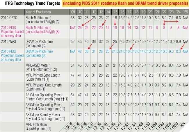
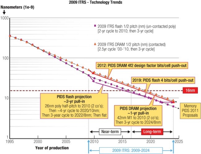
This year, half-pitch scaling was bumped up by one year from 2011 to 2010 for NAND flash and DRAM (Figures 1-2). DRAM adoption of FinFET structures is delayed by two years to 2012, vertical channels are expected in 2013, and the cell size change to 4F2 is delayed by two years. In flash memory, bit size accelerated by one year, while a transition to 3D stacking is delayed from 2014 to 2015. The change to 4 bits/cell, formerly expected in 2012, is delayed until 2019. The DRAM and flash timeline changes are included in the tables of the PIDS section of the ITRS only for 2010 but they will be proliferated to all sections and all tables in 2011.
 |
 |
At 22 nm, flash memory manufacturers will continue to use 193nm immersion with double patterning (DP) as the lithography of choice, while awaiting a mature EUV infrastructure. The key challenges for EUV remain: ensuring defect-free masks, generating adequate source brightness, and fabricating optimal resist systems. Mask metrology for EUV is nonexistent. Looking forward, to surpass 16nm patterning capability, numerical aperture (NA) will have to be increased, introducing new challenges. Incidence angles may also need to be increased, requiring thinner absorbers and mitigation of flare.
Nevertheless, the roadmap architects point out that scanner throughput has been increased dramatically, making double patterning more production worthy. With mask systems, registration and overlay have also been improved to support double patterning.
The roadmap further indicates that while flash manufacturers are likely to stick with 193nm immersion, logic and DRAM manufacturers have time to consider the alternative NGL technologies, including extending 193nm immersion DP down to a k1 of 0.15 for 22nm half pitch, maskless lithography or imprint lithography. Each of these options faces substantial core and supporting infrastructure challenges.
Front-end processes
The most substantial changes in 2010 are driven by the etch challenges for advanced CMOS devices. As gate CDs shrink, microloading among various patterns becomes more critical, requiring improved OPC modeling accuracy. The dense vs. isolated pattern etch microloading effect is critical for SiGe recess etch because the SiGe/gate distance (critical for transistor performance) strongly depends on the degree of SiGe etch microloading.
For 3D interconnect technologies, gate CD control is critical because through-silicon vias (TSV) have been shown to cause high stress, caused by the thermal expansion coefficient mismatch between copper and silicon. As a result, manufacturers may set aside a transistor exclusion zone with TSVs, which is challenging due to high transistor density.
In 2011, the front-end processes group will look closely at the introduction of multigate FETs and III/V heterogeneous integration.
Most of the 2010 changes in interconnect technology reflect the introduction of 3D integration and emerging technologies that might succeed copper/low-k approaches. A significant challenge exists in sub-2nm copper barriers, as the industry considers hybrids of Ta/Ti(N) with a thin Ru top layer. PVD and ionized PVD techniques are currently pushed to the limit because ALD still fails to demonstrate manufacturability. Regarding low-k dielectrics, air gaps (vacuum, k = 1) moved from the emerging section to a manufacturing solution and are expected to be used for kbulk < 2.0 needs. Low-k solutions going forward will be less material based and more geometry based.
Delay and power requirements in the short-term will be best addressed by 3D chip stacking with high-density TSVs as well as multicore designs. The roadmap committee has mapped out TSV geometries for global and intermediate interconnect approaches (see tables below). Global interconnect (pitches to 4-16μm) solutions are in production but intermediate level solutions (1-4μm) require further work to allow use in production.
| Global level, W2W, D2W, or D2D 3D-stacking |
2009-2012 |
2013-2015 |
| Minimum TSV diameter | 4-8µm | 2-4µm |
| Minimum TSV pitch | 8-16µm | 4-8µm |
| Minimum TSV depth | 20-50µm | 20-50µm |
| Maximum TSV aspect ratio | 5:1-10:1 | 10:1-20:1 |
| Bonding overlay accuracy | 1.0-1.5µm | 0.5-1.0µm |
| Minimum contact pitch (thermocompression) | 10µm | 5µm |
| Minimum contact pitch (solder µbump) | 20µm | 10µm |
| Number of tiers | 2-3 | 2-4 |
Intermediate interconnect level 3D-SiC Roadmap, updated
| Intermediate level, W2W 3D-stacking |
2009-2012 |
2013-2015 |
| Minimum TSV diameter | 1-2µm | 0.8-1.5µm |
| Minimum TSV pitch | 2-4µm | 1.6-3.0µm |
| Minimum TSV depth | 6-10µm | 6-10µm |
| Maximum TSV aspect ratio | 5:1-10:1 | 10:1-20:1 |
| Bonding overlay accuracy | 1.0-1.5µm | 0.5-1.0µm |
| Minimum contact pitch | 2-3µm | 2-3µm |
| Number of tiers | 2-3 | 8-16 (DRAM) |
Interestingly, an Emerging Interconnect Properties section of the ITRS is exploring first-principles of interconnect properties to determine if a combined first-level interconnect and next-generation (non-FET) switch would be most advantageous following exhaustion of the CMOS switch. Possibilities include a switch/interconnect based on carbon nanotubes or graphene.
Yield enhancement, test & packaging
In 2010, the Yield Enhancement technology working group embarked on a survey of fabs in the US, Japan, and Europe to gather defect density data for production processes and equipment. The information will be used to improve the ITRS Defect Budget and Yield Model.
One of the great testing challenges reflects the added complexity of ensuring the reliability and quality of stacked devices with TSVs. Cost containment requires creative solutions beyond testing connections and testing logic blocks and cores.
The roadmap also calls for better simulation and modeling tools for 3D packaging approaches to limit the high cost and time delay of fabricating multiple prototypes. The most difficult challenges in packaging are summarized in the table below. In 2011, readers can also look forward to expanded coverage of packaging automotive electronics, optical component packaging including optical fiber data paths, LED packaging, and photovoltaic packaging requirements.
| Assembly and packaging difficult challenges ≥16nm |
Summary of issues |
| Impact of BEOL including Cu/low-k on packaging |
|
| Wafer-level packaging |
|
| Coordinated design tools and simulators to address chip, package, and substrate co-design |
|
| Embedded components |
|
| Thinned die packaging |
|

