(January 4, 2010) — Michael A. Fury of Techcet blogs about the papers he saw at IEEE’s International Electron Device Meeting (IEDM 2010) in December. The final afternoon of IEDM (day 3, 12/08/10) continued with 4 parallel sessions and the halls and conference rooms were as crowded as they had been all week. I was compelled to spend nearly all of my time in the novel process technologies session.
Technical talks will be referenced by the assigned conference schedule number. Addi-tional information can be found online at 2010 IEDM Technical Program. All figures are reproduced with permission of IEDM.
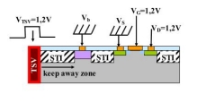
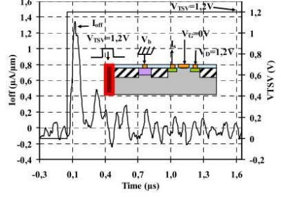
35.1: In order to quantify the impact of TSV structures on the electrical and mechanical properties of a 65nm CMOS device, H. Chaabouni of CEA LETI showed modeling and experimental work on 4µm Cu vias. Mechanical stress can affect mobility in FET devices, with PMOS being more sensitive than NMOS. This work found that a 1.7µm "keep away" zone around a TSV is needed for PMOS, none for NMOS. No effect was observed on ring oscillators as close as 5µm to the TSV. However, coupling between the TSV and FET was observed to induce a spike variation in the static NMOS drain current of up to 7µA/µm.
 |
 |
|
Figure 1. Schematic of the 2D structure used to model the TSV coupling effect on NMOS transistors (TSV/NMOS distance: 2.5µm and 5µm). A square signal is applied on the TSV. The signal is rectified with buffers before the TSV. Paper 35.1. |
Figure 2. Experimental measurement of the TSV dynamic coupling effect on the NMOS transistors leakage current (TSV/NMOS distance: 5µm). 1.4µA/µm spike variation observed. Paper 35.1. |
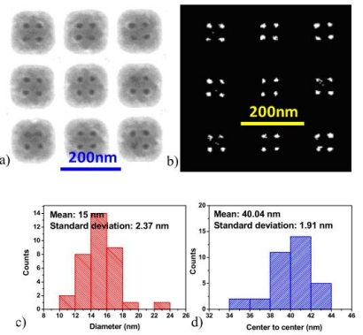
33.2: It’s amazing what’s being done with block copolymers these days. I never saw the point of them unless you were planning to make vast arrays of regularly spaced identical features. L.W. Chang at Stanford CIS showed that, with the proper placement of confinement channels and dummy structures as guide templates, you can induce directed self-assembly of reliable structures suitable for random logic designs. The work demonstrates the feasibility of processing features comparable to the natural polymer block, in this case 18nm diameters with 40nm spacing. Tweaking the template allows you to introduce additional features that would otherwise be considered outside the realm of the naturally occurring repeat pattern.
 |
 |
|
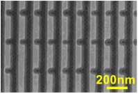
Figure 1a) Square array of self-assembled holes in square wells with 135nm side length; b) shows the binary image of a) with 36 self-assembled holes. c) and d) show the distributions of the hole diameter with average value of 40nm extracted from b). Paper 33.2. |
Figure 2. This SEM image demonstrates the formation of extra holes next to regularly packed self-assembled holes by introducing necking to the templates. Paper 33.2. |
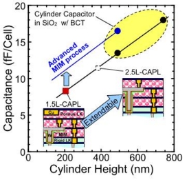
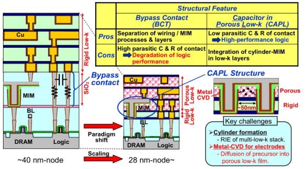
33.3: A cylindrical MIM capacitor for eDRAM in porous low-k, in which the devices are embedded in the Cu metallization layer, is proposed by K. Hijioka of Renesas Research. This naturally raises the issue of metal precursor diffusion into the low-k pores. A mo-lecular pore stack (MPS) SiCOH material with κ~2.5 and pore diameter ~0.4nm was found to be acceptable for blocking metal diffusion. TDDB of a 50nm MPS film was not degraded by CVD TiN when the MIM was integrated into 28nm eDRAM, and the MIM lifetime is projected to be >10 years. The structure is thought to be extendible to smaller nodes.
 |
|
Figure 1. Structural paradigm shift of eDRAM with cylinder-type MIM capacitors in scaled-down CMOS logics, which have porous low-k/Cu interconnects. Conventional MIM capacitors under M1-Cu need “bypass contacts (BCT),” of which the parasitic C and R increase with scaling to degrade the logic performance. Here, the researchers pro-pose a novel structure of capacitor in porous low-k film (CAPL). A key challenge is to control pore structure to keep away metal contamination in the porous low-k film during metal CVD for the MIM bottom electrode. Paper 33.3. |
|
|
|
Figure 2. Dependency of capacitance on cylinder height. Capacitance of CAPL was con-sistent to the trend of the conventional capacitor with BCT. The proposed CAPL is an extendable structure to boost the storage capacitance in the scaling eDRAM devices. Paper 33.3. |
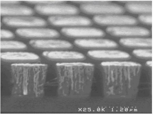
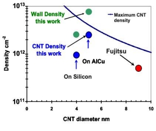
33.4: The integration of carbon nanotubes (CNT) into BEOL schemes is continuing apace. J. Dijon of CEA LITEN DTNM demonstrated CNT 1µm vias that are 10× more densely packed than previous work, and conductivity that is within engineering shouting distance of a Cu via baseline. Modeling indicates that 1013 CNT walls/cm2 are needed to meet Cu conductivity, and the present work achieved 2.5-8×10¹² walls/cm2. The 1nm diameter CNT are grown at 580°C in the via bottoms on exposed AlCu doped with Fe. These fluffy structures extend in length beyond the top of the via. They are densified by an IPA dip that shrinks the CNT ensemble to 64% of its unpacked diameter, then encapsulated with CVD Al2O3. The conductive tubes are re-exposed co-planar with the wafer surface by my old friend CMP, and top contacts are formed by liftoff. High resistivity of the via chains was attributed to contact resistance (whether top or bottom is unclear), but this seems to be a good start.
 |
 |
|
Figure 1. 1000nm (1µm) via after encapsulating CNTs with Al2O3 deposited by ALD and CMP process. Paper 33.4. |
Figure 2. State-of-the-art CNT density integrated in vias. CNT density by Fujitsu, on silicon by CEA. Green dots represent the integrated CNT wall density. Paper 33.4. |
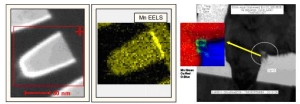
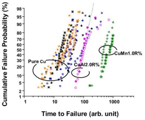
33.5: Manganese as a self-forming barrier film for Cu interconnects has been bandied about in several reincarnations since I first heard Shyam Murarka at RPI propose it in 1986. Among the current manifestations is work by T. Nogami at IBM Research, in which a CuMn seed layer with CVD Ta/TaN liner were integrated into a 32nm Cu BEOL. Data showed that CuMn had 2× the EM failure lifetime compared to CuAl with only 0.5× the at % doping level. The surface Mn is sacrificially oxidized, thus protecting the Cu surface. Optimization of the annealing process resulted in 20× more Mn at the surface while reducing the line resistance by 2×. Mn was concluded to have greater extendibility than Al for 22nm and beyond when considering future options that include Co, Ru and Ta in the barrier stack.
 |
 |
|
Figure 1. EEDL maps of segregated Cu at the Cu top surface and the damaged liner location. Paper 33.5. |
Figure 2. E-M comparison at 32nm node BEOL among pure-Cu, CuMn1.0R% and CuAl2.0R%. Paper 33.5. |
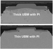
33.6: The convergence of shrinking dimensions, fragile low-k dielectrics, and the mandated replacement of PbSn solders have raised the bar for advanced flip chip interconnects. C.S. Chen of TSMC R&D presented a geometric design modification for 40 and 28nm nodes that was optimized concurrently with material modifications in the bump metallurgy, PI thickness opening, and Al pad size. A fine pitch (<150µm) Pb-free flip chip assembly solution for >400mm2 chips was shown to meet reliability specs.
 |
 |
|
Figure 1. Under-bump metallization (UBM) scheme (thick vs. thin) plays an important role in post-thermal-cycling bump integrity. After TCB1000, thick UBM with polyimide (PI) shows serious bump fatigue while thin UBM with PI does not. Paper 33.6. |
Figure 2. 3D plot on response surface of simultaneous optimization for 3 important parameters: bump size, polyimide via size, and aluminum pad size. Such a study avoids local optimization and parameters that interact with each other. Paper 33.6. |
I was quite impressed that even for the last paper of the conference, the room was still respectably full. This is indeed a serious conference!
Michael A. Fury, Ph.D, is senior technology analyst at Techcet Group, LLC, P.O. Box 29, Del Mar, CA 92014; e-mail [email protected].
Also read: IEDM Reflections
- Day 3: TSMC’s 2Xnm FinFET, and a PV+CMOS "Terminator"
- Day 3: Graphene, RRAM, MEMS, and Jedi circuit designs
- Day 2: SRO for 11nm multigate CMOS, memory updates
- Day 1: 2Xnm NAND, 3D integration, graphene FETs, biosensors
Subscribe to Solid State Technology/Advanced Packaging.
Follow Solid State Technology on Twitter.com via editors Pete Singer, twitter.com/PetesTweetsPW and Debra Vogler, twitter.com/dvogler_PV_semi.


