January 13, 2011 — Spacers are considered "conventional materials," and thus an odd topic for the cutting-edge IEEE International Electron Devices Meeting (IEDM 2010). ASM CTO Ivo Raaijmakers points out that semiconductor fab below 22nm will require different processes for spacers: atomic layer deposition (ALD) and plasma-enhanced ALD (PEALD). He speaks with Debra Vogler, senior technical editor.
Listen to Raaijmakers speak: Download (For iPhone/iPod users) or Play Now
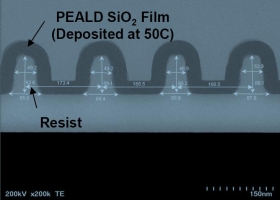
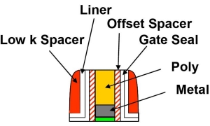
Among the reasons for using ALD/PEALD (Fig. 1) is lowering the temperature, and improving uniformity by controlling the series resistance of the device. One of the most important process knobs is chemisty choice. The Si precursor plus the nitrogen precursor, and the plasma are key parameters, explained Raaijmakers. Other important considerations include the use of a plasma and how intense that plasma is, and how much overlap you have between pulses to optimize TP in addition to optimized step coverage and layer uniformity.
|
PEALD in Production for Double
|
|
Scope of ALD Technologies
|
HKMG spacer technology
|
| Figure 1. Plasma-enhanced atomic layer deposition (PEALD) technology for spacers. SOURCE: ASM | |
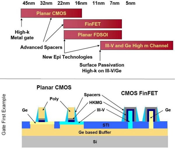
In the mid-term, Raaijmakers sees a change in architecture (FinFETs or FDSOI) (Fig. 2). For FinFETS, spacers will be even more important because of increasing aspect ratios. The transition from gate-first structures to replacement gate structures to control the workfunction will be key.
 |
| Figure 2. CMOS transistor architecture roadmap. SOURCE: ASM |
Looking even further ahead, Raaijmakers notes that the move to new channel material to III-V or pure Ge will be very involved. "We will not only have to worry about high-k and metal gate (HK+MG), but also the interface between HK+MG and III-Vs, or pure Ge, and we have to be able to passivate the surfaces," said Raaijmakers. And though the whole process integration flow will have to change to accommodate the new channel materials, Raaijmakers does not see them being introduced for another 4-6 years.
Also see: Vogler’s interview with ASM’s Glen Wilk at IEDM.
Subscribe to Solid State Technology/Advanced Packaging.
Follow Solid State Technology on Twitter.com via editors Pete Singer, twitter.com/PetesTweetsPW and Debra Vogler, twitter.com/dvogler_PV_semi.


