Nanowire-based charge-trapping memory optimized by NIST, GMU

May 23, 2011 — The National Institute of Standards and Technology (NIST) George Mason University (GMU) researchers are studying the optimal characteristics of silicon nanowires and dielectric stacks for charge-trapping memory. The resultant charge-trapping memory devices will offer lower power consumption and faster NVM operation, targeting portable computers and cell phones that operate longer between charging sessions.

NIST’s measurement capabilities were used to determine the best way to design charge-trapping memory devices based on nanowires, which must be surrounded by thin dielectric layers that store electrical charge. Software modeling and electrical device characterization led the NIST and GMU team through a range of dielectric structures to optimize device design.
Click to Enlarge
Click to Enlarge
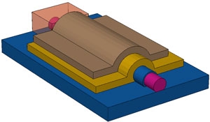
Figures. In this schematic (top) and transmission electron micrograph (TEM image, bottom), a Si nanowire is shown surrounded by a stack of thin dielectric layers. NIST scientists determined the best arrangement for this dielectric stack for the optimal construction of silicon nanowire-based memory devices. Credit: Schematic: Zhu, GMU. TEM: Bonevich, NIST.

20nm-diameter silicon nano wires form a non-volatile memory (NVM) architecture, retaining contents while power is off, much like flash memory devices. Nanowire memory devices hold an additional advantage over flash memory, which is unsuitably slow for local cache memory in the central processor. "Cache memory stores the information a microprocessor is using for the task immediately at hand," says NIST physicist Curt Richter. "It has to operate very quickly, and flash memory just isn’t fast enough."

Qiliang Li, assistant professor of Electrical and Computer Engineering at GMU, expects their findings to create a platform for more experimenters to further investigate the nanowire-based approach to high-performance NVM, leading to real applications of nanowire-based memory.

Results are published in the journal Nanotechnology:
X. Zhu, Q. Li, D. Ioannou, D. Gu, J.E. Bonevich, H. Baumgart, J. Suehle and C.A. Richter. Fabrication, characterization and simulation of high performance Si nanowire-based non-volatile memory cells. Nanotechnology, May 16, 2011, 22 254020 doi: 10.1088/0957-4484/22/25/254020. Access the article here: http://iopscience.iop.org/0957-4484/22/25/254020 
 
The National Institute of Standards and Technology (NIST) is an agency of the U.S. Department of Commerce. Learn more at http://www.nist.gov/index.html

POST A COMMENT

Easily post a comment below using your Linkedin, Twitter, Google or Facebook account. Comments won't automatically be posted to your social media accounts unless you select to share.

Nanowire-based charge-trapping memory optimized by NIST, GMU

May 23, 2011 — The National Institute of Standards and Technology (NIST) George Mason University (GMU) researchers are studying the optimal characteristics of silicon nanowires and dielectric stacks for charge-trapping memory. The resultant charge-trapping memory devices will offer lower power consumption and faster NVM operation, targeting portable computers and cell phones that operate longer between charging sessions.

NIST’s measurement capabilities were used to determine the best way to design charge-trapping memory devices based on nanowires, which must be surrounded by thin dielectric layers that store electrical charge. Software modeling and electrical device characterization led the NIST and GMU team through a range of dielectric structures to optimize device design.

Figures. In this schematic (top) and transmission electron micrograph (TEM image, bottom), a Si nanowire is shown surrounded by a stack of thin dielectric layers. NIST scientists determined the best arrangement for this dielectric stack for the optimal construction of silicon nanowire-based memory devices. Credit: Schematic: Zhu, GMU. TEM: Bonevich, NIST.

20nm-diameter silicon nano wires form a non-volatile memory (NVM) architecture, retaining contents while power is off, much like flash memory devices. Nanowire memory devices hold an additional advantage over flash memory, which is unsuitably slow for local cache memory in the central processor. "Cache memory stores the information a microprocessor is using for the task immediately at hand," says NIST physicist Curt Richter. "It has to operate very quickly, and flash memory just isn’t fast enough."

Qiliang Li, assistant professor of Electrical and Computer Engineering at GMU, expects their findings to create a platform for more experimenters to further investigate the nanowire-based approach to high-performance NVM, leading to real applications of nanowire-based memory.

Results are published in the journal Nanotechnology:
X. Zhu, Q. Li, D. Ioannou, D. Gu, J.E. Bonevich, H. Baumgart, J. Suehle and C.A. Richter. Fabrication, characterization and simulation of high performance Si nanowire-based non-volatile memory cells. Nanotechnology, May 16, 2011, 22 254020 doi: 10.1088/0957-4484/22/25/254020. Access the article here: http://iopscience.iop.org/0957-4484/22/25/254020 
 
The National Institute of Standards and Technology (NIST) is an agency of the U.S. Department of Commerce. Learn more at http://www.nist.gov/index.html

POST A COMMENT

Easily post a comment below using your Linkedin, Twitter, Google or Facebook account. Comments won't automatically be posted to your social media accounts unless you select to share.