May 10, 2011 — Novellus Systems (NASDAQ: NVLS) subsidiary Peter Wolters GmbH introduced innovative gap measurement technology for double-side silicon prime wafer polishing (DSP). New high-resolution sensors and software algorithms increase control of wafer quality, as well as throughput for the company’s AC2000-P3 system.
For precise polishing wheel control during double-side polishing, Peter Wolters incorporated several innovative features into the latest variant of the AC2000-P3 system. New contactless gauges with increased accuracy provide submicron resolution during the in-situ gap measurement. This new sensor technology has been incorporated into Peter Wolters’ upper platen adaptive control (UPAC) system and provides fast response times to process variations incurred throughout the polishing process.
 |
 |
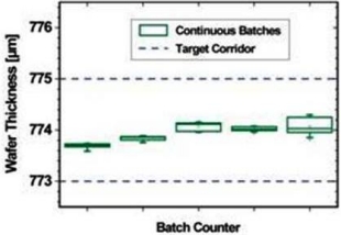
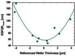
| Figure 1. Within-batch and batch-to-batch wafer thickness. | Figure 2. Low edge roll-off values (ESFQR). |
The AC2000-P3 polishing process uses a non-contact, sensor-based end point detection feature for repeatable within-batch and batch-to-batch wafer thickness (Figure 1) and low edge roll-off values (ESFQR) (Figure 2). The new sensor technology incorporates a proprietary software algorithm that replaces time-based statistical process control (SPC) to precisely measure the final wafer thickness. By eliminating non-value added polishing time, the system throughput was increased.
 |
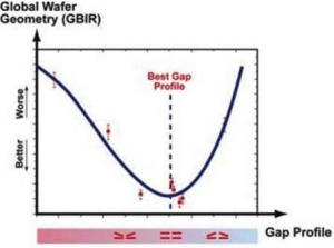
| Figure 3. Gap profile control on the GBIR measurement. |
"While designed for today’s 300mm wafers, the AC2000-P3 can also simultaneously process up to five 450mm wafers," said Dave Celli, CEO, Novellus’ Industrial Applications Group. Double-side polishing is used to manufacture 300 and 450mm prime silicon wafers for ultra-flat wafer geometries. The polishing wheel gap dimension and control throughout the polishing process is critical in determining the total within-wafer and wafer-to-wafer thickness variation (GBIR/TTV). Figure 3 shows the impact of gap profile control on the GBIR measurement, a measure of the final prime wafer quality.
Peter Wolters GmbH, part of Novellus’ Industrial Applications Group, is a leading manufacturer of high-precision surface polishing systems for substrates made of silicon, sapphire, gallium arsenide, silicon carbide and other materials used to manufacture microelectronic, micro-optical, and micromechanical devices. Peter Wolters is headquartered in Rendsburg, Germany. For more information on Peter Wolters, please visit www.peter-wolters.com
Novellus Systems Inc. (Nasdaq: NVLS) provides advanced process equipment for the global semiconductor industry. For more information, please visit www.novellus.com
Also read: Enabling 22nm litho with double-sided silicon wafer polishing process
Subscribe to Solid State Technology/Advanced Packaging.
Follow Solid State Technology on Twitter.com via editors Pete Singer, twitter.com/PetesTweetsPW and Debra Vogler, twitter.com/dvogler_PV_semi.

